Difference between revisions of "Quantar"
| Line 92: | Line 92: | ||
The SIMM has the ability to be upgraded via the SCM download procedure, but the IR SIMM and NON-IR SIMMs cannot be interchanged. This is do to the boot code being different. Using the SIMM programmer or the socketed SIMM you can reprogram the SIMM's for either. | The SIMM has the ability to be upgraded via the SCM download procedure, but the IR SIMM and NON-IR SIMMs cannot be interchanged. This is do to the boot code being different. Using the SIMM programmer or the socketed SIMM you can reprogram the SIMM's for either. | ||
| + | |||
| + | === Receivers === | ||
| + | |||
| + | {| class="wikitable sortable" | ||
| + | |- | ||
| + | ! Svc Man P/N !! CLD !! FRU P/N !! Range !! Description | ||
| + | |- | ||
| + | | TLD9831 || CLD1270 || TLN3252 || VHF R1 || [[VHF Exciter|VHF Exciter 132-154 MHz]] | ||
| + | |- | ||
| + | | TLD9832 || CLD1280 || TLN3253 || VHF R2 || [[VHF Exciter|VHF Exciter 150-174 MHz]] | ||
| + | |- | ||
| + | | CLX4000 || CLX1000 || DLN1214 || UHF R0 || [[UHF R0 Exciter|UHF Exciter 380-433 MHz]] | ||
| + | |- | ||
| + | | TLE5971 || CLE1230 || TLN3305 || UHF R1 || [[UHF Exciter|UHF Exciter 403-433 MHz]] | ||
| + | |- | ||
| + | | TLE5972 || CLE1240 || TLN3306 || UHF R2 || [[UHF Exciter|UHF Exciter 438-470 MHz]] | ||
| + | |- | ||
| + | | TLE5973 || CLE1210 || TLN3375 || UHF R3 || [[UHF Exciter|UHF Exciter 470-490 MHz]] | ||
| + | |- | ||
| + | | TLE5974 || CLE1220 || TLN3376 || UHF R4 || [[UHF Exciter|UHF Exciter 490-520 MHz]] | ||
| + | |- | ||
| + | | TLF6930 || CLF1520 || TLN3308 || 900 || [[900 MHz Exciter|900 MHz Exciter 935-941 MHz]] | ||
| + | |} | ||
| + | |||
| + | |||
=== Exciter === | === Exciter === | ||
Revision as of 01:33, 28 November 2015
Quantar/Quantro info
There is a bunch of info here about the technical aspects of the Quantar Stations
Programming
Links to programming stuff
CSS 007.13.R022.0035 for EPIC4 Smart Zone SCM
WinRSS 14.08.01 Current Windows RSS
Firmware
SIMM Images
Conventional Firmware for U1-U4 on the SIMM module 20.14.048
IntelliRepeater (IR) Firmware for U1-U8 on the two bank SIMM module 20.14.520
Wireline Images
Wireline 20.10.816 for AT27C010 Chips. This works with the 20.14.048 Conventional Firmware
Exciter Images
This is the matching Exciter Image for a AM27C512 UV EPROM
Code Plug format
Manuals
Hardware info
Part numbers
Here are part numbers and what the correspond to
Station Control info
Station Control Module or SCM is the heart of the Quantar station. The SCM comes in different revisons known as EPIC.
- EPIC I - TTN4094
- EPIC II
- EPIC III
- EPIC IV - This is only for the Smart Zone trunking. IT will not work for conventional
- EPIC V
The only difference between the various versions of the EPICs (excluding EPIC IV) is the hardware is newer. There is no difference in functionality for conventional analog/astro/P25 operation.
SIMM info
The SIMM used for firmware in the Quantar EPIC 2/3 is an 80 pin SIMM and is basically unobtanimum. The conventional uses 4, 29F040 chips arranged to be 32 bits wide. This means each chip stores every 4th byte.
Example we store "QUANTAR MOTOROLA" in the SIMM
| Chip 1 | Chip 2 | Chip 3 | Chip 4 |
|---|---|---|---|
| Q | U | A | N |
| T | A | R | |
| M | O | T | O |
| R | O | L | A |
So if we read Chip 1 we'd see QTMR.
The IR uses a two bank SIMM with the same layout (8 chips total)
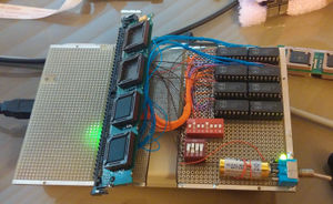
It's possible to pull these chips and read/write them if you have the right programmer. Taking advantage of this I was able to build a SIMM programmer for the soldered in place SIMM's that essentially programs one chip at a time (8bits).
It's not pretty but it works.
The SIMM has the ability to be upgraded via the SCM download procedure, but the IR SIMM and NON-IR SIMMs cannot be interchanged. This is do to the boot code being different. Using the SIMM programmer or the socketed SIMM you can reprogram the SIMM's for either.
Receivers
| Svc Man P/N | CLD | FRU P/N | Range | Description |
|---|---|---|---|---|
| TLD9831 | CLD1270 | TLN3252 | VHF R1 | VHF Exciter 132-154 MHz |
| TLD9832 | CLD1280 | TLN3253 | VHF R2 | VHF Exciter 150-174 MHz |
| CLX4000 | CLX1000 | DLN1214 | UHF R0 | UHF Exciter 380-433 MHz |
| TLE5971 | CLE1230 | TLN3305 | UHF R1 | UHF Exciter 403-433 MHz |
| TLE5972 | CLE1240 | TLN3306 | UHF R2 | UHF Exciter 438-470 MHz |
| TLE5973 | CLE1210 | TLN3375 | UHF R3 | UHF Exciter 470-490 MHz |
| TLE5974 | CLE1220 | TLN3376 | UHF R4 | UHF Exciter 490-520 MHz |
| TLF6930 | CLF1520 | TLN3308 | 900 | 900 MHz Exciter 935-941 MHz |
Exciter
The exciters contain their own CPU which communicates with the SCM over a SPI bus. This CPU runs it's own firmware and requires a socketed UV EPROM to upgrade it. This also controls the PA meeting and the bit of EEPROM in the CPU stores the alignment settings for the exciter and PA. Generally a Exciter/PA pair will not need to be realigned if moved from one chassis to another, although it should be checked.
| Svc Man P/N | CLD | FRU P/N | Range | Description |
|---|---|---|---|---|
| TLD9831 | CLD1270 | TLN3252 | VHF R1 | VHF Exciter 132-154 MHz |
| TLD9832 | CLD1280 | TLN3253 | VHF R2 | VHF Exciter 150-174 MHz |
| CLX4000 | CLX1000 | DLN1214 | UHF R0 | UHF Exciter 380-433 MHz |
| TLE5971 | CLE1230 | TLN3305 | UHF R1 | UHF Exciter 403-433 MHz |
| TLE5972 | CLE1240 | TLN3306 | UHF R2 | UHF Exciter 438-470 MHz |
| TLE5973 | CLE1210 | TLN3375 | UHF R3 | UHF Exciter 470-490 MHz |
| TLE5974 | CLE1220 | TLN3376 | UHF R4 | UHF Exciter 490-520 MHz |
| TLF6930 | CLF1520 | TLN3308 | 900 | 900 MHz Exciter 935-941 MHz |
Troof Table
There is a ID code representing the exciter type, it consists of R3700 to R3710. These are either pull up or down resistors on a 6 bit code and are identified on the schematic on the left side of U3700, the μP. Below is the table in MSB-LSB format, with a 1 being high (5v) and a 0 being a low (0v).
| Dip switch! | Band! | Binary! | Notes in the RSS! |
|---|---|---|---|
| 0 | VHF_R1 | 000000 | |
| 1 | VHF_R2 | 000001 | VHF R2 SL |
| 2 | UHF_R1 | 000010 | |
| 3 | UHF_R2 | 000011 | |
| 4 | 800 | 000100 | |
| 5 | VHF_R3 | 000101 | sl |
| 6 | VHF_R4 | 000110 | |
| 7 | VHF_R1 | 000111 | |
| 8 | VHF_R2 | 001000 | VHF R2 FL |
| 9 | VHF_R3 | 001001 | |
| 10 | VHF_R4 | 001010 | |
| 11 | 900 | 001011 | |
| 12 | UHF_R3 | 001100 | |
| 13 | UHF_R4 | 001101 | |
| 14 | blank | 001110 | |
| 15 | blank | 001111 | |
| 16 | blank | 010000 | |
| 17 | blank | 010001 | |
| 18 | blank | 010010 | |
| 19 | blank | 010011 | uhf r0 from book |
| 20 | blank | 010100 | |
| 21 | blank | 010101 | |
| 22 | blank | 010110 | |
| 23 | blank | 010111 | |
| 24 | blank | 011000 | |
| 25 | blank | 011001 | |
| 26 | blank | 011010 | |
| 27 | blank | 011011 | |
| 28 | blank | 011100 | |
| 29 | blank | 011101 | |
| 30 | blank | 011110 | |
| 31 | blank | 011111 | |
| 32 | blank | 100000 | |
| 33 | blank | 100001 | |
| 34 | blank | 100010 | |
| 35 | blank | 100011 | |
| 36 | blank | 100100 | |
| 37 | blank | 100101 | boot |
| 38 | blank | 100110 | |
| 39 | blank | 100111 | |
| 40 | blank | 101000 | |
| 41 | blank | 101001 | |
| 42 | blank | 101010 | |
| 43 | blank | 101011 | |
| 44 | blank | 101100 | |
| 45 | blank | 101101 | |
| 46 | blank | 101110 | |
| 47 | blank | 101111 | "RSS only" |
| 48 | blank | 110000 | |
| 49 | blank | 110001 | |
| 50 | blank | 110010 | |
| 51 | blank | 110011 | |
| 52 | blank | 110100 | RAP says VHF_R2 SL |
| 53 | blank | 110101 | |
| 54 | blank | 110110 | |
| 55 | blank | 110111 | |
| 56 | blank | 111000 | |
| 57 | blank | 111001 | |
| 58 | blank | 111010 | |
| 59 | blank | 111011 | |
| 60 | blank | 111100 | |
| 61 | blank | 111101 | |
| 62 | blank | 111110 | |
| 63 | INVALID | 111111 | Exciter is in reset all LED's are on and the PA fans turn on |
Power Amp
The power amps are actually a cool design.
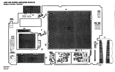
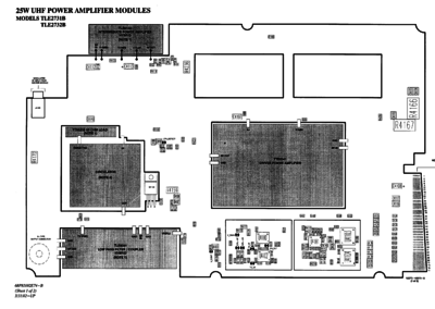
Their are two basic power amps, a 25W, and a 100/110/125w (depending on band). The power amps all use the same general board layout, with the frequency dependent parts separate from the support components. The 25W PA is a passively cooled unit with a massive heatsink, while the 100/110/125W unit has active cooling with a horizontal heatsink and two cooling fans moving air front to back.
There are a couple different revisions of the PA's so the main PCB has changed a bit over time.
[[|thumbnail|center]]
The PA doesn't contain any CPU, it's controlled via the exciter CPU with basic analog level lines going over to the exciter. Some of what's measured by the exciter
- Intermediate PA drive level - this is the output of the IPA to the final PA pallet
- Driver PA Level - output of the final PA before the circulator (FPA_DETECT).
- TX Power Forward - Output measured at the output of the Low Pass Filter
- TX Power Reverse - Reflected Power from the antenna port
- OMNI voltage - this is the control voltage on the IPA which comes from the SCM as a 0-5V control signal (V_CONT). This 0-5v controls a transistor making a 0-14v signal to provide the gain of the IPA. This is the basis of the power control. The Control Voltage from the SCM is only present during keydown.
- IPA Current detect
- DPA Side A & B current sense
- Temperature of the PA
- Fan on/off and alarm
- PA_ID bits A & B - resistor divider that programs to reference voltages in .5v increments to ID the PA hardware to the exciter.
All these are measured over an TDM bus that selects each at a 200ms interval using a single analog input on the exciter CPU.
PA types
| Svc Man P/N | Other P/N | Rated Power | Range | Description |
|---|---|---|---|---|
| CTX1146 | DLN1216 | 110 | UHF R0 | Second Generation UHF PA 380-433 MHz |
| TTE2061 | TLN3444 | 110 | UHF R1 | First Generation UHF PA 403-433 MHz |
| CLE6164 | Example | 110 | UHF R1 | Second Generation UHF PA 403-433 MHz |
| TTE2062 | TLN3446 | 110 | UHF R2 | First Generation UHF PA 438-470 MHz |
| CLE6165 | CLE1308 | 110 | UHF R2 | Second Generation UHF PA 438-470 MHz |
| TTE2063 | 110 | UHF R3 | First Generation UHF PA 470-490 MHz | |
| TTE6373 | 110 | UHF R3 | Second Generation UHF PA 470-490 MHz | |
| TTE2064 | 100 | UHF R4 | First Generation UHF PA 490-520 MHz | |
| TTE6374 | 100 | UHF R4 | Second Generation UHF PA 490-520 MHz |
| PA Type | PA_ID_A | PA_ID_B | R4162 | R4163 | R4164 | R4165 | Official? |
|---|---|---|---|---|---|---|---|
| 900 100W | 3.0 | .5 | 20.5k | 10k | 1k | OPEN | YES |
| 800 100W | 0.5 | 1.0 | OPEN | 0 | 1.5K | 15K | YES |
| 800 20W | 0.0 | 1.0 | OPEN | 1k | 1.5K | 15K | YES |
| UHF 110W R0 | 0.0 | 1.5 | OPEN | 0 | 390 | 1k | YES |
| UHF 110W R1 | 1.0 | 0.5 | 15k | 1.5k | 560 | 10k | YES |
| UHF 110W R2 | 1.5 | 0.5 | 1k | 390 | 100 | 1k | YES |
| UHF 110W R3 | 3.0 | 1.0 | 2.2k | 2.7k | 1.5k | 15k | YES |
| UHF 100W R4 | 3.5 | 1.0 | 18k | 15k | 1.5k | 15k | YES |
| UHF 25W R1 | 5.0 | 0.0 | 33.2k | OPEN | 0 | OPEN | YES |
| UHF 25W R2 | 0.0 | 0.5 | OPEN | 0 | 1k | OPEN | YES |
| VHF 125W R1 | 3.0 | 0.0 | 20.5k | 10k | 0 | OPEN | YES |
| VHF 125W R2 | 0.0 | 0.0 | OPEN | 0 | 0 | OPEN | YES |
| VHF 25W R1/R2 | 4.5 | 0.0 | 12k | 68k | 0 | OPEN | YES |
| VHF 25W R1 | 3.5 | 0.0 | NO |
UHF 110W Generation 1 UHF 110W Generation 2
CTF1091A 100 W 800 MHz
CTF1092A 100 W 900 MHz
CTX1146A Range 0 Power Amplifier
TLF1800B 100W Power Amplifier Module
TLF1930C 100W Power Amplifier Module
TLF1940B 20W Power Amplifier Module
TTE2061A 110W Power Amplifier UHF R1
TTE2062A 110W Power Amplifier UHF R2
TTE2063A 110W Power Amplifier UHF R3
TTE2064A 110W Power Amplifier UHF R4
TLE2511A/ 110W Power Amplifier Module TLE2512A TLE2521 TLE2572 TLE2731B 25W Power Amplifier Module UHF R1 TLE2732B 25W Power Amplifier Module UHF R2 TLD3101G 125W Power Amplifier Module VHF R1 TLD3102G 125W Power Amplifier Module VHF R2 TLD3110C 25W Power Amplifier Module VHF R1/R2 CLX4002A 100/110W Power Amplifier Module (UHF; R1-R4) CLE6164A 100/110W Power Amplifier CLE6165A Module (UHF; R1-R4)
TTE6373A/ 100/110W Power Amplifier TTE6374A Module (UHF; R1-R4)
Conversions
Work in progress on moving Qunatar bands
Going to move this to the various exciter/PA/receiver pages verses having its own page.
VHF R2 to R1
Looks like it should work
Exciter
Parts difference and re-tune the VCO's
Amplifier
25W PA
This covers both R1 and R2.
125W PA MODELS TLD3101/TLD3102
The 125W PA is the same PA pallet, Low Pass Filter, and IPA. The circulator is different, and about 300 from MOTO. Should be a matter of changing the ID bits
CLD1298 and CLD1299 newer 125W PA's look like they are them same.
VHF R2 to 220 MHz
Software works, it's putting the R4 code plug in, verified the 212.5 cross over frequency for the VCO's. Still need to work out some bugs in it. Should use the 800 MHz for the 220 MHz programing.
Exciter is working.
PA is a complete rebuild, working on it, circulator is being reworked. The A+B voltage feeds are a problem. Right now it keys up, and then shits the bed as the PA is fail. I've tested it by putting good voltage on the IPA, PA, FPA and SWR sense lines. Still doesn't like the PA not drawing current and craps out after like 30 seconds, but it was long enough to test the output from the exciter, it's 13.5 dBm on the Rigol.
Receiver VCO is working, need to modify the image filter and test.
UHF R0 to R2
This is doable
Exciter
Power AMP
Receiver
UHF R1 to R2
Converting the R1 (403-433) to R2 (438-470)
I've done a number of these that all meet spec. If your planing on a conversion it's the best to start with, due to PA isolator covering it, and it being easier to remove material from the preselector than add it.
I've never done a R3 or R4 to R2, I'd like to though.
the R0 is easy as well, but it's got a different design to the VCO's.
Exciter
- Test it first! Trying to modify a broken exciter is like pushing a rope.
- Remove the board from the case and take off the covers.
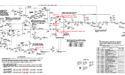
- Now locate the VCOs (IC3200). These are sealed units and have no diagram. Check out the schematic! The Diagram is wrong when it shows the upper and lower VCO!
- 4 Looking at the VCO I find it's easier to remove the copper shield than try to desolder the entire VCO module.
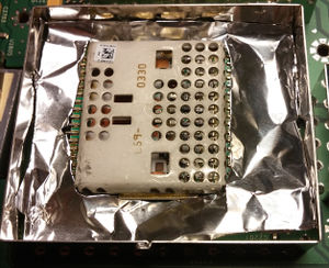
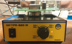
The VCO substrate is ceramic high K board. It's sensitive to thermal shock, so be careful about this, as it will crack. It's sicking noise. The best way to remove the VCO shield is using chip quick on the "pins" under the board and then flipping it over and using a preheater on the underside for 3-4 min at 450°f.
Prior to preheating I fashion supports out of Aluminum foil or other material and jam them between the PCB and the underside of the VCO. This will prevent the VCO board from falling off it's pins when removing the shield. Once this is done, mask off the area using hole cut in some foil. This is a heat shield for the other parts of the board.
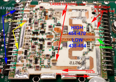
Now turn on the preheater and wait for the board to warm up. Once it's up to 450° F take a hot air wand set to 15 l/min of flow and 650°f to the shield. After about 2-3 min it will loosen and you can pull the shield straight up. Careful you don't disturb any of the VCO parts, as they will most likely be reflowed too. If you do, don't panic, just look at the before picture and put everything back to how it was on the VCO. It's a pretty easy circuit to figure out.
Once you have the VCO exposed you can attach test wires to it. You'll need the following points
- 8.5 V power to high and low VCO (not at the same time, just tack the wire on)
- 0-12 V on the steering line
- output loops of wire on the VCO output. These are to be looped around a probe and into a spectrum anaylizer to view the output.
First a couple things about the VCO's,
- with the shield on they move up about 2.5 MHz
- from hot to cold Fr changes about 1.5 to 2 MHz. Hotter makes Fr go down, cool makes it go up.
- removing capacitance makes Fr go up.
- removing inductance makes Fr go up.
- the sweet spot for the VCO steering voltage os 2.5-7.5 v
- each VCO is designed to cover half the range of the quantar.
- * The Exciter will change VCO's when it hits it's center frequency +25khz. You can verify this my looking at the steering voltage in the exciter as you change frequencies. A test config file (Codeplug) makes this easy.
Starting with the low VCO, hook it up and sweep the 0-12v supply to check it's 385-430 MHz. within 5 MHz is ok, this VCO only covers 16 MHz in operation.
- put 5.5v on the steering line.
We're going to align it for a CF of 444 MHz. The reason for this is the lower VCO covers 438-454, making the center 446, but with the shield off we will see the CF be ~2 MHz lower. The shield adds capacitance to the circuit and this ups the resonte frequency.
With the voltage on the steering line, cut a 75 mill strip of .250 copper foil. It's not critical, you'll be adjusting it. Place it on the VCO Trombone to short out part of the stripline. You can safely monitor the output of the VCO and move this at the same time. I've found it's best to shoot lower than 444 MHz. Once you are within a few MHz, let the board cool. You'll find the Fr rising as it cools. Moving the short closer to the trombone end lowers Fr, pulling it further away from the end raises Fr.
- now while monitoring the VCO output on the spectrum anyliser, use a dimond tip dremmel grinder and remove some of the high impediance end tuning cap on the vco. Go a very little at a time, it makes a big difference. Use this to bring the VCO frequency up to 444 MHz on the dot. It's normal for the VCO to jump a couple hundred KHZ or so depending on the stability of your power supply. There is no PLL running to lock it.
- now lets test the VCO with the cover off you should see the following (give or take a few MHZ). Keep in mind with the shield in place you'll see the frequency go up about 2 MHz.
| Voltage | Low | High |
|---|---|---|
| .8 | 425 | 442 |
| 5.5 | 444 | 460 |
| 9.2 | 461 | 477 |
The VCO is most happy running at 2.5 to 7.5 volts, and needs to cover 438-454 and 454-470. So long as it covers this range in between 2.5 to 7.5 Volts it will work. there is a bit more space on the low end than the high end, so if it runs at 2v at for 438 vs 2.5v for 438 MHz, it's not a concern. Keep in mind the Fr is lower with the cover off, so if it's 1v at 438 while tuning it, there is a good chance it will not lock with the case on.
- After the Lower VCO is modified, modify the high one.
Remove the 8.5v from the Low VCO and put it on the high VCO line and hook up your spectrum analyzer on the output. Verify the existing tuning range of 406-440 from 0 to 10v. It's normal to see spurs near the 0 and 12v steering levels.
Once it's working correctly and you see the upper VCO, you need to do the same procedure as the low vco.
With 5.5v on the steering line, and add a .075 with copper strip on the trombone side of the VCO tank. We need to align this to a bit lower (.5 to 1 MHz) than center frequency of 460 (again we're expecting this to be 462 MHz with the cover on the VCO). This allows us to peek the VCO right onto 460 MHz by trimming up the capacitor with a Dremel.
Allow the VCO to cool and verify the high tuning range between 2.5 and 7.5 of 452-468 (454-470 with case on). Again it's not critical, but we need to have this be in the center of the total VCO range to keep things linear.
- Change the Exciter Modulation input
The Quantar has a splatter filter on the modulation input on the VCO's. What we've done makes the VCO a bit more sensitive to modulation input and while the Quantar can calibrate up to a 10khz deviation on the test level, in some cases we see >10khz of deviation. The soultion to this is a resistor change in the voltage divider of R3250/R3251.
- Changing R3250 from 10k to 16k seams to reliably resolve this. It's a 5% 0805 size part, and very easy to work with.
- Change the exciter ID.
As you can see in the Table above, we need the change the ID from R1 to R2. This is a simple 1 resistor move.
- Move R3700 to R3701
- additional changes
Technically two more parts need to be changed, C3112 and C3277 need to be changed from 3.3 to 2.7 pF. I've not changed these and found all output to be right on the money. You're welcome to change them if you have 0805 size 2.7 pF caps on hand.
Once this is all done, it's time to put the VCO shield back on.
- make sure you clean up the VCO PCB with flux remover first.
- ensure you have all the Chipquick removed from the bottom holes in the PCB.
- Solder the PCB holes in place first
- use a small tip to solder the shield back on the VCO.
- You can verify the tuning range once again if you so choose. In alignment I test the exciter with a test code plug and use the built in volt meter to monitor it.
Now reassemble the entire PCB in the chassis and put the shields back in place. It's a good time to upgrade the firmware too.
- Put the exciter back in the chassis and hook it up to the PA. For the first part of this testing we will only look at the steering voltage of the VCO as reported in the RSS. We don't need to engage the transmitter as the VCO will run all the time the exciter is on.
- Setup a test code plug with the following in it.
| Channel | Frequency | Voltage |
|---|---|---|
| 1. | 420.00 | |
| 2. | 425.00 | |
| 3. | 430.00 | |
| 4. | 435.00 | |
| 5. | 438.00 | 2.5 |
| 6. | 454.00 | 7.0 |
| 7. | 454.25 | 2.5 |
| 8. | 470.00 | 7.0 |
| 9. | 475.00 | |
| 10. | 480.00 | |
| 11. | 485.00 | |
| 12. | 490.00 | |
| 13. | 495.00 | |
| 14. | 500.00 |
Check that the switch over happens at 454.25 MHz. Again you want the voltages to be as close as possible, but even a volt off is not a huge deal so long as you're over 1v and under 8v for the maximum and minimum.
- once this is verified, it's time to align the exciter. This writes the data in to the exciter CPU internal EEPROM.
The deviation and linearity need to be aligned. The exciter will calibrate the deviation of every mode once the exciter is setup. Note the frequencies used, you're aligning the minimum and maximum of each VCO.
Power AMP
Receiver
| Part number | R1 | R2 | function |
| C2050 | 9.1 pF | 8.2 pF | |
| C2051 | 16pF | 13pF | |
| C2053 | 18 pF | 16 pF | |
| C2054 | 8.2 pF | 6.8 pF | |
| C2057 | 18 pF | 16 pF | |
| C2059 | 18 pF | 13 pF | |
| C2070 | 5.6 pF | 3.3 pF | |
| C2076 | 7.54 pF | 5.6 pF | |
| C2079 | 9.1 pF | 5.6 pF | |
| C2083 | 47 pF | 22 pF | |
| R2449 | 0 Ohm | 0 Ohm | ID |
| R2450 | 0 Ohm | 3300 Ohm | ID |
