Difference between revisions of "V.24 Level Shifter Board"
| (30 intermediate revisions by the same user not shown) | |||
| Line 1: | Line 1: | ||
[[Category:Quantar]] | [[Category:Quantar]] | ||
| + | [[Category:Wireline]] | ||
| + | [[Category:Astro-Tac]] | ||
| + | [[Category:v.24]] | ||
| − | This is a page about the v.24 level converter I made to be fully drop in replacement for the OEM board. | + | This is a page about the v.24 level converter I made to be fully drop in replacement for the [[Wireline#v.24_TTN4010|TTN4010 OEM board]]. |
| + | |||
| + | '''[https://store.w3axl.com/products/w9cr-v-24-wireline-level-shifter W3AXL has them for sale if you're interested in buying them]''' | ||
| + | <div style=float:left;> | ||
| + | __TOC__ | ||
| + | </div> | ||
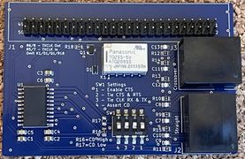
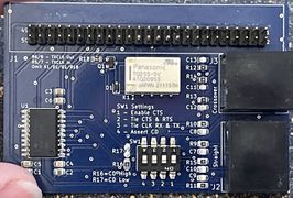
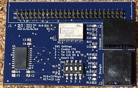
| + | [[File:2024-05-22 Front Complete.jpg|thumb|400px|right|W9CR v.24 Board v2024-05-22]] | ||
| + | <div style="clear: both"></div> | ||
| + | |||
| + | I designed this as the OEM v.24 daughter-card boards are hard to find and pricey when they are available. Other aftermarket boards such as the [[Dave NX4Y v.24 Board]] have limitations which make them unsuitable for my needs such as not supporting clocking in both directions. My design supports every thing the OEM board does and adds several additional features. It also lies nearly flat in either port of the Wireline Board. | ||
= Features = | = Features = | ||
* '''Full OEM Compatibility''' - This will work in place of the OEM board | * '''Full OEM Compatibility''' - This will work in place of the OEM board | ||
| − | ** Includes a relay so that the station can originate clock | + | ** Includes a relay so that the station can originate clock '''''OR''''' be clocked by DCE. |
* Simple design - Affordable and easy to assemble, only one IC | * Simple design - Affordable and easy to assemble, only one IC | ||
* The following can be done via dip switch at the RS232 level | * The following can be done via dip switch at the RS232 level | ||
| Line 12: | Line 24: | ||
** Tie TXCLK and RXCLK together - this allows a station to connect to another which is set to not send TX clock | ** Tie TXCLK and RXCLK together - this allows a station to connect to another which is set to not send TX clock | ||
** Tie CTS and RTS together - needed in some cases for certain v24 to DCE connections | ** Tie CTS and RTS together - needed in some cases for certain v24 to DCE connections | ||
| − | * Built in cross over port to connect two stations | + | * Built in cross over port to connect two stations with a standard Ethernet patch cable without needing a crossover adapter. |
| − | * Internally ESD ( | + | ** This simplifies making the DB25 to RJ-45 dongles for interconnecting with Cisco routers as there is no need for tying signal lines together in the dongle. |
| − | * Fits in the front or back ports of the Wireline board without contacting or putting pressure on other | + | * Internally ESD (10kv) protected design - meets or exceeds the OEM v.24 daughter card or other designs based on the MC145406 |
| − | * Not a Graham Cracker | + | * RF bypass caps on all RS232 Lines |
| + | * Fits in the front or back ports of the Wireline board without contacting or putting pressure on other components on the wireline board. | ||
| + | ** Using the AMP connector there is about 100 mils extra clearance. | ||
| + | [[File:v.24 with AMP connector on wireline showing clerence from front.jpg|thumb|300px|right|Clerence with amp connector]] | ||
| + | * Permits adding v.24 interface to quantars without the need to replace/modify faceplate. Cables can be routed out the back. | ||
| + | * Builtin v.24 network tap for debugging (both RJ-45's are connected to the lines.) | ||
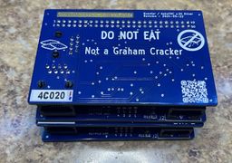
| + | * Not a Graham Cracker | ||
| + | <div style="clear: both"></div> | ||
== Tested Config == | == Tested Config == | ||
* Quantar/Quantro base station | * Quantar/Quantro base station | ||
* PDR3500 Base station | * PDR3500 Base station | ||
| − | * AstroTAC 3000 Comparator <ref> | + | * AstroTAC 3000 Comparator <ref>this needs the CD line asserted</ref> |
Tested with TRN7477, TRN7667, CLN6955, CLN6956 and CLN7343 wireline boards. | Tested with TRN7477, TRN7667, CLN6955, CLN6956 and CLN7343 wireline boards. | ||
| + | |||
| + | = Notes = | ||
| + | |||
| + | J1 on the board was designed to take a mating AMP connector for the wireline board. Using this however presents a problem as it needs to be modified. All production boards use a simple 2x25 100 mil pitch connector (as the OEM does) to simplify this. | ||
| + | |||
| + | The Astro-Tac 3000 needs CD active to put the port active. | ||
| + | |||
| + | == Connectors == | ||
| + | Using an Ethernet patch cable plugged into the straight on one side and plugged into the cross on the other is the preferred way to connect two stations. Both stations can be set to send clock, but in the event one is set to have it's TX provided by the other (quantar's RX clock is always external) the SW1-3 can be set on to loop the clock lines. | ||
| + | |||
| + | |||
| + | '''Straight Through Connector''' | ||
| + | {| class="wikitable" style="vertical-align:bottom;" | ||
| + | |- style="font-weight:bold; text-align:center;" | ||
| + | ! colspan="4" | Quantar/ATAC OEM v.24 | ||
| + | |- | ||
| + | | RJ45 | ||
| + | | Color | ||
| + | | Function | ||
| + | | Mot v.24 Board | ||
| + | |- | ||
| + | | style="text-align:right; background-color:#F90; color:#FFF;" | 1 | ||
| + | | style="background-color:#F90; color:#FFF;" | W/Orange | ||
| + | | Tx Clock | ||
| + | | style="text-align:right;" | 1 | ||
| + | |- | ||
| + | | style="text-align:right; background-color:#F90;" | 2 | ||
| + | | style="background-color:#F90;" | Orange | ||
| + | | CD | ||
| + | | style="text-align:right;" | 2 | ||
| + | |- | ||
| + | | style="text-align:right; background-color:#38761D; color:#FFF;" | 3 | ||
| + | | style="background-color:#38761D; color:#FFF;" | W/Green | ||
| + | | Rx Clock | ||
| + | | style="text-align:right;" | 3 | ||
| + | |- | ||
| + | | style="text-align:right; background-color:#15C;" | 4 | ||
| + | | style="background-color:#15C;" | Blue | ||
| + | | GRND | ||
| + | | style="text-align:right;" | 4 | ||
| + | |- | ||
| + | | style="text-align:right; background-color:#15C; color:#FFF;" | 5 | ||
| + | | style="background-color:#15C; color:#FFF;" | W/Blue | ||
| + | | Tx Data | ||
| + | | style="text-align:right;" | 5 | ||
| + | |- | ||
| + | | style="text-align:right; background-color:#38761D;" | 6 | ||
| + | | style="background-color:#38761D;" | Green | ||
| + | | Rx Data | ||
| + | | style="text-align:right;" | 6 | ||
| + | |- | ||
| + | | style="text-align:right; background-color:#B45F06; color:#FFF;" | 7 | ||
| + | | style="background-color:#B45F06; color:#FFF;" | W/Brown | ||
| + | | RTS | ||
| + | | style="text-align:right;" | 7 | ||
| + | |- | ||
| + | | style="text-align:right; background-color:#B45F06;" | 8 | ||
| + | | style="background-color:#B45F06;" | Brown | ||
| + | | CTS | ||
| + | | style="text-align:right;" | 8 | ||
| + | |} | ||
| + | |||
| + | '''Crossover Port''' | ||
| + | {| class="wikitable" style="vertical-align:bottom;" | ||
| + | |- style="font-weight:bold; text-align:center;" | ||
| + | ! colspan="4" | Crossover v.24 | ||
| + | |- | ||
| + | | RJ45 | ||
| + | | Color | ||
| + | | Function | ||
| + | | Mot v.24 Board | ||
| + | |- | ||
| + | | style="text-align:right; background-color:#F90; color:#FFF;" | 1 | ||
| + | | style="background-color:#F90; color:#FFF;" | W/Orange | ||
| + | | Rx Clock | ||
| + | | style="text-align:right;" | 3 | ||
| + | |- | ||
| + | | style="text-align:right; background-color:#F90;" | 2 | ||
| + | | style="background-color:#F90;" | Orange | ||
| + | | CD | ||
| + | | style="text-align:right;" | 2 | ||
| + | |- | ||
| + | | style="text-align:right; background-color:#38761D; color:#FFF;" | 3 | ||
| + | | style="background-color:#38761D; color:#FFF;" | W/Green | ||
| + | | Tx Clock | ||
| + | | style="text-align:right;" | 1 | ||
| + | |- | ||
| + | | style="text-align:right; background-color:#15C;" | 4 | ||
| + | | style="background-color:#15C;" | Blue | ||
| + | | GRND | ||
| + | | style="text-align:right;" | 4 | ||
| + | |- | ||
| + | | style="text-align:right; background-color:#15C; color:#FFF;" | 5 | ||
| + | | style="background-color:#15C; color:#FFF;" | W/Blue | ||
| + | | Rx Data | ||
| + | | style="text-align:right;" | 6 | ||
| + | |- | ||
| + | | style="text-align:right; background-color:#38761D;" | 6 | ||
| + | | style="background-color:#38761D;" | Green | ||
| + | | Tx Data | ||
| + | | style="text-align:right;" | 5 | ||
| + | |- | ||
| + | | style="text-align:right; background-color:#B45F06; color:#FFF;" | 7 | ||
| + | | style="background-color:#B45F06; color:#FFF;" | W/Brown | ||
| + | | CTS | ||
| + | | style="text-align:right;" | 8 | ||
| + | |- | ||
| + | | style="text-align:right; background-color:#B45F06;" | 8 | ||
| + | | style="background-color:#B45F06;" | Brown | ||
| + | | RTS | ||
| + | | style="text-align:right;" | 7 | ||
| + | |} | ||
| + | |||
| + | === CISCO DCE === | ||
| + | |||
| + | Connecting to a CISCO router DCE DB25F is easily done with a DB25M to RJ45 adapter using the following pin out. What is nice is the DB25-rj45 adapter requires no internal splicing of logic lines like the prior boards do. | ||
| + | |||
| + | {| class="wikitable" style="vertical-align:bottom;" | ||
| + | |- style="font-weight:bold; text-align:center;" | ||
| + | ! colspan="4" | Straight to Cisco DCE | ||
| + | |- | ||
| + | | RJ45 | ||
| + | | Color | ||
| + | | Function | ||
| + | | DB25 Male | ||
| + | |- | ||
| + | | style="text-align:right; background-color:#4A86E8;" | 1 | ||
| + | | style="background-color:#4A86E8;" | Blue | ||
| + | | Rx Clock | ||
| + | | style="text-align:right;" | 17 | ||
| + | |- | ||
| + | | style="text-align:right; background-color:#F90;" | 2 | ||
| + | | style="background-color:#F90;" | Orange | ||
| + | | CD | ||
| + | | style="text-align:right;" | 20 | ||
| + | |- | ||
| + | | style="text-align:right; color:#FFF;background-color:#000" | 3 | ||
| + | | style="color:#FFF;background-color:#000" | Black | ||
| + | | Tx Clock | ||
| + | | style="text-align:right;" | 15 | ||
| + | |- | ||
| + | | style="text-align:right; background-color:#F00;" | 4 | ||
| + | | style="background-color:#F00;" | Red | ||
| + | | GRND | ||
| + | | style="text-align:right;" | 7 | ||
| + | |- | ||
| + | | style="text-align:right; background-color:#0F0;" | 5 | ||
| + | | style="background-color:#0F0;" | Green | ||
| + | | Rx Data | ||
| + | | style="text-align:right;" | 3 | ||
| + | |- | ||
| + | | style="text-align:right; background-color:#FF0;" | 6 | ||
| + | | style="background-color:#FF0;" | Yellow | ||
| + | | Tx Data | ||
| + | | style="text-align:right;" | 2 | ||
| + | |- | ||
| + | | style="text-align:right; background-color:#B45F06;" | 7 | ||
| + | | style="background-color:#B45F06;" | Brown | ||
| + | | CTS | ||
| + | | style="text-align:right;" | 5 | ||
| + | |- | ||
| + | | style="text-align:right;" | 8 | ||
| + | | White | ||
| + | | RTS | ||
| + | | style="text-align:right;" | 4 | ||
| + | |} | ||
| + | |||
| + | DIP Switches: 1, 4 | ||
| + | Clock: Quantar takes clock from Cisco | ||
| + | DB-25 Male to RJ45 | ||
| + | Uses Ethernet straight through patch cable | ||
| + | Cisco provides Clock on TX and RX | ||
| + | Cisco sends CTS and quantar sends RTS | ||
| + | Cisco needs CD active | ||
| + | |||
| + | Verified 2024-06-26 | ||
| + | |||
| + | [[File:v.24 straight to Cisco DCE DB25M.jpg|400px|Right|DB25 wireing]] | ||
| + | <div style="clear: both"></div> | ||
| + | |||
| + | = DIP Switches = | ||
| + | SW1 provides the following options: | ||
| + | |||
| + | 1 - Enable CTS connection from RJ-45 to wireline, normally ON (same as on OEM board) | ||
| + | 2 - Tie CTS and RTS (at RS232 level) | ||
| + | 3 - Tie TX and RX clock (at RS232 level | ||
| + | 4 - Assert CD Active High (R16 can be swapped to R17 if this must be active low) | ||
| + | |||
| + | = Docs = | ||
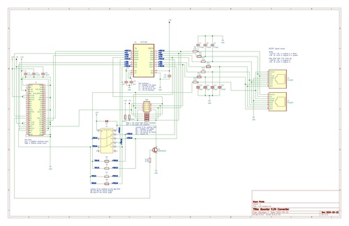
| + | == Diagram == | ||
| + | [[File:2024-05-22 Diagram of v.24 board.pdf|page=1|500px|link=https://wiki.w9cr.net/images/7/74/2024-05-22_Diagram_of_v.24_board.pdf|2024-05-22 Diagram of v.24 board]] | ||
= Background info = | = Background info = | ||
https://www.ti.com/lit/an/slla544/slla544.pdf | https://www.ti.com/lit/an/slla544/slla544.pdf | ||
| + | |||
| + | https://www.ti.com/lit/ds/symlink/sn75185.pdf | ||
https://www.analog.com/en/resources/technical-articles/fundamentals-of-rs232-serial-communications.html | https://www.analog.com/en/resources/technical-articles/fundamentals-of-rs232-serial-communications.html | ||
| Line 34: | Line 246: | ||
https://www.analog.com/media/en/technical-documentation/data-sheets/MAX3185.pdf | https://www.analog.com/media/en/technical-documentation/data-sheets/MAX3185.pdf | ||
| + | |||
| + | '''Maxim datasheet has the pin-out wrong on page 5 for the T3IN and T1IN lines.''' This is being resolved, but T3 is 13 and T1 is 16 with the chips i have. This also matches the SN75185 chip that it's designed as drop in replacement for. | ||
good: | good: | ||
| Line 40: | Line 254: | ||
https://www.ti.com/lit/ds/symlink/tl145406.pdf | https://www.ti.com/lit/ds/symlink/tl145406.pdf | ||
| + | |||
| + | Cisco cable pinouts for rs232 | ||
| + | |||
| + | https://www.cisco.com/c/en/us/td/docs/routers/access/hardware/notes/marcabl.html#pgfId-43546 | ||
| + | |||
| + | = Revisions = | ||
| + | |||
| + | == 2024-05-22 == | ||
| + | Expected to work 100%, in beta testing now. Switched to the SN75185 part and updated the layout. | ||
| + | |||
| + | <gallery mode=packed widths=300px> | ||
| + | 2024-05-22 Front Complete.jpg|2024-05-22 Front | ||
| + | 2024-05-22 Back Complete.jpg|2024-05-22 Reverse | ||
| + | 2024-05-22 all complete.jpg | ||
| + | 2024-05-22 completed.jpg | ||
| + | 2024-05-22 dickbutt.jpg | ||
| + | 2024-05-22 first 4 completed.jpg | ||
| + | </gallery> | ||
| + | |||
| + | I did find it much easier to use a solder pot to solder the through the hole parts. This made my idea for untented vias (no solder mask over them) and the name in exposed copper a rather poor choice. I was able to use a cheap vinyl cutter and cut some kapton tape. Next revision will be designed for manufacturing. | ||
| + | |||
| + | [[File:v.24 boards ready to be dipped.jpg|thumb|400px|center|Boards ready to be dipped]] | ||
| + | <div style="clear: both"></div> | ||
| + | |||
| + | == 2024-05-12 == | ||
| + | |||
| + | Discovered the MAX3185 datasheet has pins 13 and 16 swapped on it. All the CAD models have the same swap. After cutting and fixing this, the board works as expected. | ||
| + | |||
| + | Analog devices confirmed the datasheet is incorrect. Note this is a over 30 year old datasheet. I've decided to move the to the TI part, which functions the same for the most part. | ||
| + | |||
| + | I was able to fix a couple for testing and verify they work as intended once this mod is done. This will need a board re-spin. | ||
| + | |||
| + | <gallery mode=packed widths=300px> | ||
| + | v.24 2024-05-12 back.jpg | ||
| + | v.24 2024-05-12 with AMP connector fixed.jpg | ||
| + | </gallery> | ||
| + | |||
| + | == 2024-05-01 == | ||
| + | |||
| + | PCB needs to be respun; IO ports are reversed on the IO lines of the level converter. | ||
| + | |||
| + | Change the switch to use RS232 levels vs 5v TTL levels for 2-4. | ||
| + | |||
| + | <gallery mode=packed widths=300px> | ||
| + | Quantar Extention cables on wireline modified chassis.jpg | ||
| + | v.24 2024-05-01 all soldered.jpg | ||
| + | v.24 2024-05-01 back.jpg | ||
| + | v.24 2024-05-01 front.jpg | ||
| + | v.24 2024-05-01 oh shit! wires.jpg | ||
| + | v.24 2024-05-01 on wireline testing.jpg | ||
| + | v.24 2024-05-01 ready to reflow.jpg | ||
| + | </gallery> | ||
| + | |||
| + | = Production Testing = | ||
| + | |||
| + | With Quantar set to originate clock | ||
| + | |||
| + | * plug in board, relay should activate | ||
| + | * Verify clock is seen on the TXCLK pin 3 (W/Green) of J2 or pin 1 (W/Orange) of J3. | ||
| + | * Close SW3 and check for clock on RXCLK (W/Orange) of J2 | ||
| + | * Connect using straight through cable from cross port to astrotac v.24 port set to clock from DCE. Check that it is down, but you see data on the TXD line. | ||
| + | * close SW1 to enable CTS and check that Pin 42 CTS of J1 is low and that CTS on J2 is RS232 level high (4-10v) | ||
| + | * close SW2 to tie RTS and CTS and check that RTS and CTS are low on J1 (41 and 42) | ||
| + | * close SW4 to assert CD and see that the link is up between quantar and astrotac. | ||
| + | |||
| + | This should verify everything other than TXCLK input from DCE. | ||
Latest revision as of 22:06, 28 July 2024
This is a page about the v.24 level converter I made to be fully drop in replacement for the TTN4010 OEM board.
W3AXL has them for sale if you're interested in buying them

I designed this as the OEM v.24 daughter-card boards are hard to find and pricey when they are available. Other aftermarket boards such as the Dave NX4Y v.24 Board have limitations which make them unsuitable for my needs such as not supporting clocking in both directions. My design supports every thing the OEM board does and adds several additional features. It also lies nearly flat in either port of the Wireline Board.
Features
- Full OEM Compatibility - This will work in place of the OEM board
- Includes a relay so that the station can originate clock OR be clocked by DCE.
- Simple design - Affordable and easy to assemble, only one IC
- The following can be done via dip switch at the RS232 level
- CD asserted and tied to MARK or SPACE
- Tie TXCLK and RXCLK together - this allows a station to connect to another which is set to not send TX clock
- Tie CTS and RTS together - needed in some cases for certain v24 to DCE connections
- Built in cross over port to connect two stations with a standard Ethernet patch cable without needing a crossover adapter.
- This simplifies making the DB25 to RJ-45 dongles for interconnecting with Cisco routers as there is no need for tying signal lines together in the dongle.
- Internally ESD (10kv) protected design - meets or exceeds the OEM v.24 daughter card or other designs based on the MC145406
- RF bypass caps on all RS232 Lines
- Fits in the front or back ports of the Wireline board without contacting or putting pressure on other components on the wireline board.
- Using the AMP connector there is about 100 mils extra clearance.

- Permits adding v.24 interface to quantars without the need to replace/modify faceplate. Cables can be routed out the back.
- Builtin v.24 network tap for debugging (both RJ-45's are connected to the lines.)
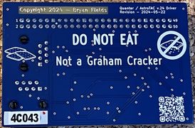
- Not a Graham Cracker
Tested Config
- Quantar/Quantro base station
- PDR3500 Base station
- AstroTAC 3000 Comparator [1]
Tested with TRN7477, TRN7667, CLN6955, CLN6956 and CLN7343 wireline boards.
Notes
J1 on the board was designed to take a mating AMP connector for the wireline board. Using this however presents a problem as it needs to be modified. All production boards use a simple 2x25 100 mil pitch connector (as the OEM does) to simplify this.
The Astro-Tac 3000 needs CD active to put the port active.
Connectors
Using an Ethernet patch cable plugged into the straight on one side and plugged into the cross on the other is the preferred way to connect two stations. Both stations can be set to send clock, but in the event one is set to have it's TX provided by the other (quantar's RX clock is always external) the SW1-3 can be set on to loop the clock lines.
Straight Through Connector
| Quantar/ATAC OEM v.24 | |||
|---|---|---|---|
| RJ45 | Color | Function | Mot v.24 Board |
| 1 | W/Orange | Tx Clock | 1 |
| 2 | Orange | CD | 2 |
| 3 | W/Green | Rx Clock | 3 |
| 4 | Blue | GRND | 4 |
| 5 | W/Blue | Tx Data | 5 |
| 6 | Green | Rx Data | 6 |
| 7 | W/Brown | RTS | 7 |
| 8 | Brown | CTS | 8 |
Crossover Port
| Crossover v.24 | |||
|---|---|---|---|
| RJ45 | Color | Function | Mot v.24 Board |
| 1 | W/Orange | Rx Clock | 3 |
| 2 | Orange | CD | 2 |
| 3 | W/Green | Tx Clock | 1 |
| 4 | Blue | GRND | 4 |
| 5 | W/Blue | Rx Data | 6 |
| 6 | Green | Tx Data | 5 |
| 7 | W/Brown | CTS | 8 |
| 8 | Brown | RTS | 7 |
CISCO DCE
Connecting to a CISCO router DCE DB25F is easily done with a DB25M to RJ45 adapter using the following pin out. What is nice is the DB25-rj45 adapter requires no internal splicing of logic lines like the prior boards do.
| Straight to Cisco DCE | |||
|---|---|---|---|
| RJ45 | Color | Function | DB25 Male |
| 1 | Blue | Rx Clock | 17 |
| 2 | Orange | CD | 20 |
| 3 | Black | Tx Clock | 15 |
| 4 | Red | GRND | 7 |
| 5 | Green | Rx Data | 3 |
| 6 | Yellow | Tx Data | 2 |
| 7 | Brown | CTS | 5 |
| 8 | White | RTS | 4 |
DIP Switches: 1, 4
Clock: Quantar takes clock from Cisco
DB-25 Male to RJ45
Uses Ethernet straight through patch cable
Cisco provides Clock on TX and RX
Cisco sends CTS and quantar sends RTS
Cisco needs CD active

Verified 2024-06-26

DIP Switches
SW1 provides the following options:
1 - Enable CTS connection from RJ-45 to wireline, normally ON (same as on OEM board)
2 - Tie CTS and RTS (at RS232 level)
3 - Tie TX and RX clock (at RS232 level
4 - Assert CD Active High (R16 can be swapped to R17 if this must be active low)
Docs
Diagram
Background info
https://www.ti.com/lit/an/slla544/slla544.pdf
https://www.ti.com/lit/ds/symlink/sn75185.pdf
https://www.analog.com/en/products/max3185.html
https://www.analog.com/media/en/technical-documentation/data-sheets/MAX3185.pdf
Maxim datasheet has the pin-out wrong on page 5 for the T3IN and T1IN lines. This is being resolved, but T3 is 13 and T1 is 16 with the chips i have. This also matches the SN75185 chip that it's designed as drop in replacement for.
good:
https://electronics.stackexchange.com/a/649122
https://www.ti.com/lit/ds/symlink/tl145406.pdf
Cisco cable pinouts for rs232
https://www.cisco.com/c/en/us/td/docs/routers/access/hardware/notes/marcabl.html#pgfId-43546
Revisions
2024-05-22
Expected to work 100%, in beta testing now. Switched to the SN75185 part and updated the layout.
2024-05-22 Front
2024-05-22 Reverse


I did find it much easier to use a solder pot to solder the through the hole parts. This made my idea for untented vias (no solder mask over them) and the name in exposed copper a rather poor choice. I was able to use a cheap vinyl cutter and cut some kapton tape. Next revision will be designed for manufacturing.

2024-05-12
Discovered the MAX3185 datasheet has pins 13 and 16 swapped on it. All the CAD models have the same swap. After cutting and fixing this, the board works as expected.
Analog devices confirmed the datasheet is incorrect. Note this is a over 30 year old datasheet. I've decided to move the to the TI part, which functions the same for the most part.
I was able to fix a couple for testing and verify they work as intended once this mod is done. This will need a board re-spin.


2024-05-01
PCB needs to be respun; IO ports are reversed on the IO lines of the level converter.
Change the switch to use RS232 levels vs 5v TTL levels for 2-4.


Production Testing
With Quantar set to originate clock
- plug in board, relay should activate
- Verify clock is seen on the TXCLK pin 3 (W/Green) of J2 or pin 1 (W/Orange) of J3.
- Close SW3 and check for clock on RXCLK (W/Orange) of J2
- Connect using straight through cable from cross port to astrotac v.24 port set to clock from DCE. Check that it is down, but you see data on the TXD line.
- close SW1 to enable CTS and check that Pin 42 CTS of J1 is low and that CTS on J2 is RS232 level high (4-10v)
- close SW2 to tie RTS and CTS and check that RTS and CTS are low on J1 (41 and 42)
- close SW4 to assert CD and see that the link is up between quantar and astrotac.
This should verify everything other than TXCLK input from DCE.
- ↑ this needs the CD line asserted