Difference between revisions of "UHF Receiver"
| (35 intermediate revisions by the same user not shown) | |||
| Line 1: | Line 1: | ||
| − | This page covers the Range 1 to Range 4 receivers. The Range 0 is a newer (and easier to modify) design. | + | This page covers the Range 1 to Range 4 receivers. The [[UHF R0 Receiver|Range 0]] is a newer (and easier to modify) design. |
= Basics = | = Basics = | ||
| Line 9: | Line 9: | ||
1128152131.jpg|UHF RX Back | 1128152131.jpg|UHF RX Back | ||
1128152130a.jpg|UHF RX Case | 1128152130a.jpg|UHF RX Case | ||
| − | + | 1128152131a.jpg|UHF RX Internal | |
</gallery> | </gallery> | ||
| + | The receiver is a high side injection with the 1st Lo operating +73.35 MHz higher than the receiver frequency. | ||
| + | The SCM knows what type of module is inserted by reading voltage divider resistors on the u2600 A/D Converter. | ||
| + | Some of these are on ports used for other things, Change Frequency and Lock and then A8 input is used for ID. Note the resistors have the same labels on the UHF boards but on other bands the same parts have different labels. The R2606 and R2607 form a voltage divider feeding the A8 input with the computed voltage in volts. | ||
| + | {| class="wikitable" | ||
| + | !Range!!R2449 Chg Freq!!R2450 Lock!! SPACE !!R2606!!R2607!!A8 Volts | ||
| + | |- | ||
| + | |UHF R0||0||3300||||5600||3300||1.9 | ||
| + | |- | ||
| + | |UHF R1||0||0||||1200||1200||2.5 | ||
| + | |- | ||
| + | |UHF R2||0||3300||||1200||1200||2.5 | ||
| + | |- | ||
| + | |UHF R3||3300||0||||1200||1200||2.5 | ||
| + | |- | ||
| + | |UHF R4||3300||3300||||1200||1200||2.5 | ||
| + | |- | ||
| + | !VHF!!R2413!!R2415!!!!R2812!!R2814!! | ||
| + | |- | ||
| + | |VHF R1||0||0||||2700||1200||1.5 | ||
| + | |- | ||
| + | |VHF R2||0||3300||||2700||1200||1.5 | ||
| + | |- | ||
| + | !800/900!!R2422!!R2414!!!!R2816!!R2815!! | ||
| + | |- | ||
| + | |900||0||0||||1200||4700||4.0 | ||
| + | |- | ||
| + | |800||0||0||||1200||2700||3.5 | ||
| + | |} | ||
| − | |||
| − | [[ | + | The service manual excerpt is in PDF and below. |
| − | + | ||
| − | + | [[media:UHF Receiver Models TRE6281-TRE6282-TRE6283-TRE6284.pdf|UHF Receiver Models TRE6281-TRE6282-TRE6283-TRE6284 Service Manual Excerpt]] | |
| − | [[File:UHF Receiver Models TRE6281-TRE6282-TRE6283-TRE6284-4.png|thumb|UHF | + | |
| + | In PNG format. | ||
| + | <gallery heights=100px widths=100px mode="packed"> | ||
| + | UHF Receiver Models TRE6281-TRE6282-TRE6283-TRE6284-1.png|Schematic Sheet 1 of 4 | ||
| + | UHF Receiver Models TRE6281-TRE6282-TRE6283-TRE6284-2.png|Schematic Sheet 2 of 4 | ||
| + | UHF Receiver Models TRE6281-TRE6282-TRE6283-TRE6284-3.png|Schematic Sheet 3 of 4 | ||
| + | UHF Receiver Models TRE6281-TRE6282-TRE6283-TRE6284-4.png|Schematic Sheet 4 of 4 | ||
| + | </gallery> | ||
| + | |||
| + | Note on the schematic the VCO high and Low are reversed. This seems to be a recurring theme in the Quantar manuals. | ||
| + | [[File:UHF Receiver Models TRE6281-TRE6282-TRE6283-TRE6284 VCO correction schematic.png|thumb|Reversed VCO's]] | ||
| + | |||
| + | As the VCO runs at 73.35 MHz higher than the intended receive frequency the VCO will expect to lock over the following ranges. The ideal spot for the VCO to operate is between 2.5 and 7.5 Volts highlighted in pink below. | ||
| + | |||
| + | {| class="wikitable" | ||
| + | !Range !!colspan="5" style="text-align: center;"|Lower VCO!! colspan="5" style="text-align: center;"|Upper VCO | ||
| + | |- | ||
| + | |Volts||0.8||style="background:Pink"|2.5||style="background:pink"|5.0||style="background:pink"|7.5||9.2||0.8||style="background:pink"|2.5||style="background:Pink"|5.0||style="background:pink"|7.5||9.2 | ||
| + | |- | ||
| + | |UHF R1||462||style="background:Pink"|467||style="background:Pink"|479||style="background:Pink"|491||499||478||style="background:Pink"|491||style="background:Pink"|499||style="background:Pink"|506||514 | ||
| + | |- | ||
| + | |UHF R2||498||style="background:Pink"|511||style="background:Pink"|519||style="background:Pink"|527||536||514||style="background:Pink"|527||style="background:Pink"|535||style="background:Pink"|543||552 | ||
| + | |- | ||
| + | |UHF R3||528||style="background:Pink"|543||style="background:Pink"|549||style="background:Pink"|555||564||541||style="background:Pink"|555||style="background:Pink"|561||style="background:Pink"|567||575 | ||
| + | |- | ||
| + | |UHF R4||553||style="background:Pink"|567||style="background:Pink"|574||style="background:Pink"|580||589||568||style="background:Pink"|580||style="background:Pink"|587||style="background:Pink"|593||601 | ||
| + | |} | ||
| + | |||
| + | The VCO is much like the VCO in the exciter, a sealed unit with no further diagram available from the factory. | ||
| + | |||
| + | <gallery heights=100px widths=100px mode="packed-hover"> | ||
| + | UHF R2 RX VCO Case on.jpg|UHF R2 RX VCO Case on | ||
| + | UHF R2 RX VCO case off.jpg|UHF R2 RX VCO case off | ||
| + | RX VCO case off up close.jpg|UHF R2 VCO Close up | ||
| + | </gallery> | ||
| + | |||
| + | = Conversions = | ||
| + | |||
| + | Converting the boards | ||
| + | |||
| + | This is changing, I have a better way, [[Quantar UHF RX conversion|old method]]. | ||
| + | |||
| + | |||
| + | |||
| + | == R1 to R2 == | ||
| + | |||
| + | This is the conversion we're focused on as there are tons of 403-433 MHz (US Federal) Range 1 units on the market for cheap. | ||
| + | |||
| + | In general you should have the following to work on this: | ||
| + | |||
| + | * Soldering iron with fine tip (Metcal suggested) | ||
| + | * Hot air station | ||
| + | * Under board heater | ||
| + | * Small tools/tweezers | ||
| + | * Silicone rubber stock cut to support the underside of the VCO. | ||
| + | * Flux, and other small parts for rework | ||
| + | * Quantar [[Quantar Backplane Extender|backplane extender cables]] (PCI extender cables cut down to fit) | ||
| + | * '''A clear understanding of how the VCO's work and how the PLL operates''' | ||
| + | * Quantar programmed up with the [[Quantar Test Codeplugs|test code plug]]. | ||
| + | |||
| + | Almost needed, you really should have it, but can do without: | ||
| + | |||
| + | * Voltmeter - You can use the WINRSS metering screen to view the steering level of the VCO. It's a pain to switch back and forth, but it can be done. | ||
| + | * Service monitor/SINAD meter - If you don't have a meter you can use a known weak signal to do a 20db quieting test. | ||
| + | * RJ-9 speaker to SINAD meter input cable. | ||
| + | |||
| + | Nice to have: | ||
| + | |||
| + | * Bench DVM | ||
| + | * Bench PSU | ||
| + | * Spectrum Analyzer and probes | ||
| + | |||
| + | === Parts needed === | ||
| + | |||
| + | You will need the following parts for this. Note the capacitors which are critical in terms of value are noted. If you find that sensitivity is off, suspect that you got the wrong value of caps here, 1-2 dB will be noticeable. | ||
| + | |||
| + | {| class="wikitable" | ||
| + | |- | ||
| + | ! Value | ||
| + | ! Tolerence | ||
| + | ! Part(s) | ||
| + | ! Digikey partnumber | ||
| + | ! Size | ||
| + | |- | ||
| + | | 3.3 | ||
| + | | +-0.1pf 50v | ||
| + | | C2070 | ||
| + | | 732-12216 | ||
| + | | 0805 | ||
| + | |- | ||
| + | | 5.6 | ||
| + | | +-0.25pf 50v | ||
| + | | C2076, C2079 | ||
| + | | 478-KGM21BCG2A5R6CT-ND | ||
| + | | 0805 | ||
| + | |- | ||
| + | | 6.8 | ||
| + | | +-0.1pf 50v | ||
| + | | C2054 | ||
| + | | 478-KGM21BCG2A6R8DTCT-ND | ||
| + | | 0805 | ||
| + | |- | ||
| + | | 8.2 | ||
| + | | +-0.1pf 50v | ||
| + | | C2050 | ||
| + | | 732-12219-1-ND | ||
| + | | 0805 | ||
| + | |- | ||
| + | | 13 | ||
| + | | +-2pf 50v | ||
| + | | C2051, C2059 | ||
| + | | 478-10374-1-ND | ||
| + | | 0805 | ||
| + | |- | ||
| + | | 16 | ||
| + | | +-2pf 50v | ||
| + | | C2053, C2057 | ||
| + | | 478-10377-1-ND | ||
| + | | 0805 | ||
| + | |- | ||
| + | | 22 | ||
| + | | 5% 50v | ||
| + | | C2083 | ||
| + | | 478-KGM21BCG2A220JTCT-ND | ||
| + | | 0805 | ||
| + | |- | ||
| + | | 3300 | ||
| + | | 5% 1/8 watt | ||
| + | | R2450 | ||
| + | | RMCF0805JT3K30CT-ND | ||
| + | | 0805 | ||
| + | |} | ||
| + | |||
| + | === Procedure Overview === | ||
| + | |||
| + | In general the VCO (both) need to be moved up in frequency and the image filters from the mixer need to be moved up by changing some chip caps. The ID resistors of the board must be changed to identify the receiver as Range 2 as well. Prior procedures required a bunch of manual power supplies, sweeping the circuit, and monitoring with a spectrum analyzer. This procedure uses the Quantar to control the receiver as it's being worked on using an [[Quantar Backplane Extender|extender cable]]. | ||
| + | |||
| + | The VCO must be modified so that it's able to lock from 2.5 to 7.5v. The steering voltage actually is usable from .95 to 8.95v, but tempeture will affect the resonance of the VCO, and so you want to have the high and low frequency to be at 2.5 - 7.5 volts giving enough room on each side for environmental variations. | ||
| + | |||
| + | === Preparation === | ||
| + | |||
| + | First lets prep the setup and get some notes on the receiver before we move it. | ||
| + | |||
| + | Setup the Quantar and install the extender cables. | ||
| + | |||
| + | Remove the receiver from it's housing. | ||
| + | |||
| + | Install the board in the work holder/vise. | ||
| + | |||
| + | Hook it up to the backplane and program in the '''Range 1 test codeplug'''. | ||
| + | |||
| + | Sweep and record the VCO steering voltage on each channel where it locks. If not using a voltmeter, you can use the measurement screen in RSS to see the steering level. This is very important as it gives a base line of performance on the receiver before modification. | ||
| + | |||
| + | Note that if you're using a volt meter on the VCO steering line, it will not receive properly. Ensure you do that separate from the SINAD testing. | ||
| + | |||
| + | {| class="wikitable" style="text-align:right; vertical-align:bottom;" | ||
| + | |- style="font-weight:bold; text-align:center;" | ||
| + | ! style="text-align:left;" | | ||
| + | ! colspan="8" | Lower VCO | ||
| + | ! colspan="8" style="background-color:#FFF;" | Upper VCO | ||
| + | |- style="font-weight:bold;" | ||
| + | | style="text-align:left;" | Channel | ||
| + | | 1 | ||
| + | | 2 | ||
| + | | 3 | ||
| + | | 4 | ||
| + | | 5 | ||
| + | | style="background-color:#F4CCCC;" | 6 | ||
| + | | style="background-color:#F4CCCC;" | 7 | ||
| + | | style="background-color:#F4CCCC;" | 8 | ||
| + | | style="background-color:#F4CCCC;" | 9 | ||
| + | | style="background-color:#F4CCCC;" | 10 | ||
| + | | style="background-color:#F4CCCC;" | 11 | ||
| + | | 12 | ||
| + | | 13 | ||
| + | | 14 | ||
| + | | 15 | ||
| + | | 16 | ||
| + | |- style="font-weight:bold;" | ||
| + | | style="text-align:left;" | R1 | ||
| + | | 384.5250 | ||
| + | | 388.2250 | ||
| + | | 391.9250 | ||
| + | | 395.6250 | ||
| + | | 399.3250 | ||
| + | | style="background-color:#F4CCCC;" | 403.0250 | ||
| + | | style="background-color:#F4CCCC;" | 410.5000 | ||
| + | | style="background-color:#F4CCCC;" | 417.9750 | ||
| + | | style="background-color:#F4CCCC;" | 418.0250 | ||
| + | | style="background-color:#F4CCCC;" | 425.5000 | ||
| + | | style="background-color:#F4CCCC;" | 432.9750 | ||
| + | | 436.8000 | ||
| + | | 440.6250 | ||
| + | | 444.4500 | ||
| + | | 448.2750 | ||
| + | | 452.1000 | ||
| + | |- style="font-weight:bold;" | ||
| + | | style="text-align:left;" | R2 | ||
| + | | 417.9000 | ||
| + | | 421.9250 | ||
| + | | 425.9500 | ||
| + | | 429.9750 | ||
| + | | 434.0000 | ||
| + | | style="background-color:#F4CCCC;" | 438.0250 | ||
| + | | style="background-color:#F4CCCC;" | 446.0000 | ||
| + | | style="background-color:#F4CCCC;" | 453.9750 | ||
| + | | style="background-color:#F4CCCC;" | 454.0250 | ||
| + | | style="background-color:#F4CCCC;" | 462.0000 | ||
| + | | style="background-color:#F4CCCC;" | 469.9750 | ||
| + | | 474.1250 | ||
| + | | 478.2750 | ||
| + | | 482.4250 | ||
| + | | 486.5750 | ||
| + | | 490.7250 | ||
| + | |- | ||
| + | | style="text-align:left;" | R1 Shield on | ||
| + | | UNLOCK | ||
| + | | UNLOCK | ||
| + | | 1.813 | ||
| + | | 2.504 | ||
| + | | 3.248 | ||
| + | | style="background-color:#F4CCCC;" | 4.029 | ||
| + | | style="background-color:#F4CCCC;" | 5.678 | ||
| + | | style="background-color:#F4CCCC;" | 7.379 | ||
| + | | style="background-color:#F4CCCC;" | 3.843 | ||
| + | | style="background-color:#F4CCCC;" | 5.495 | ||
| + | | style="background-color:#F4CCCC;" | 7.204 | ||
| + | | 8.089 | ||
| + | | 8.982 | ||
| + | | UNLOCK | ||
| + | | UNLOCK | ||
| + | | UNLOCK | ||
| + | |- | ||
| + | | style="text-align:left;" | R1 Shield Off | ||
| + | | UNLOCK | ||
| + | | 1.808 | ||
| + | | 2.480 | ||
| + | | 3.203 | ||
| + | | 3.962 | ||
| + | | style="background-color:#F4CCCC;" | 4.743 | ||
| + | | style="background-color:#F4CCCC;" | 6.376 | ||
| + | | style="background-color:#F4CCCC;" | 8.045 | ||
| + | | style="background-color:#F4CCCC;" | 4.735 | ||
| + | | style="background-color:#F4CCCC;" | 6.395 | ||
| + | | style="background-color:#F4CCCC;" | 8.084 | ||
| + | | 8.959 | ||
| + | | UNLOCK | ||
| + | | UNLOCK | ||
| + | | UNLOCK | ||
| + | | UNLOCK | ||
| + | |- | ||
| + | | style="text-align:left;" | Delta | ||
| + | | style="text-align:left;" | | ||
| + | | style="text-align:left;" | | ||
| + | | 0.667 | ||
| + | | 0.699 | ||
| + | | 0.714 | ||
| + | | style="background-color:#F4CCCC;" | 0.714 | ||
| + | | style="background-color:#F4CCCC;" | 0.698 | ||
| + | | style="background-color:#F4CCCC;" | 0.666 | ||
| + | | style="background-color:#F4CCCC;" | 0.892 | ||
| + | | style="background-color:#F4CCCC;" | 0.900 | ||
| + | | style="background-color:#F4CCCC;" | 0.880 | ||
| + | | 0.870 | ||
| + | | style="text-align:left;" | | ||
| + | | style="text-align:left;" | | ||
| + | | style="text-align:left;" | | ||
| + | | style="text-align:left;" | | ||
| + | |- | ||
| + | | style="text-align:left;" | R1 SINAD | ||
| + | | style="text-align:left;" | | ||
| + | | style="text-align:left;" | | ||
| + | | -120.1 | ||
| + | | -120.1 | ||
| + | | -120.0 | ||
| + | | style="background-color:#F4CCCC;" | -120.1 | ||
| + | | style="background-color:#F4CCCC;" | -120.1 | ||
| + | | style="background-color:#F4CCCC;" | -120.2 | ||
| + | | style="background-color:#F4CCCC;" | -120.0 | ||
| + | | style="background-color:#F4CCCC;" | -120.0 | ||
| + | | style="background-color:#F4CCCC;" | -120.0 | ||
| + | | -119.4 | ||
| + | | 119.4 | ||
| + | | style="text-align:left;" | | ||
| + | | style="text-align:left;" | | ||
| + | | style="text-align:left;" | | ||
| + | |- | ||
| + | | style="text-align:left;" | R2 Shield On | ||
| + | | UNLOCK | ||
| + | | UNLOCK | ||
| + | | 1.328 | ||
| + | | 2.056 | ||
| + | | 2.876 | ||
| + | | style="background-color:#F4CCCC;" | 3.766 | ||
| + | | style="background-color:#F4CCCC;" | 5.680 | ||
| + | | style="background-color:#F4CCCC;" | 7.727 | ||
| + | | style="background-color:#F4CCCC;" | 2.319 | ||
| + | | style="background-color:#F4CCCC;" | 4.001 | ||
| + | | style="background-color:#F4CCCC;" | 5.890 | ||
| + | | 6.920 | ||
| + | | 7.968 | ||
| + | | 9.027 | ||
| + | | UNLOCK | ||
| + | | UNLOCK | ||
| + | |- | ||
| + | | style="text-align:left;" | R2 SINAD | ||
| + | | style="text-align:left;" | | ||
| + | | style="text-align:left;" | | ||
| + | | | ||
| + | | | ||
| + | | | ||
| + | | style="background-color:#F4CCCC;" | | ||
| + | | style="background-color:#F4CCCC;" | | ||
| + | | style="background-color:#F4CCCC;" | | ||
| + | | style="background-color:#F4CCCC;" | | ||
| + | | style="background-color:#F4CCCC;" | | ||
| + | | style="background-color:#F4CCCC;" | | ||
| + | | | ||
| + | | | ||
| + | | | ||
| + | | style="text-align:left;" | | ||
| + | | style="text-align:left;" | | ||
| + | |} | ||
| + | |||
| + | === VCO Modification === | ||
| + | |||
| + | This is very critical circuit to work on and is a sealed ceramic unit. Motorola used unique VCO's for each band range, however the Range 1 can be modified using some "stub" lines of copper foil to bring it's frequency up. This is complicated as the unit is soldered in place and has a heavy plated steel cover soldered over it. | ||
| + | |||
| + | ==== Prepare the VCO for rework ==== | ||
| + | |||
| + | The VCO shield must be removed, but as the entire VCO will be reflowed at the same time, it will "fall" off the headers holding it off the board. This is solved by using some 1/4 inch wide 60 mil thick silicone stock. Fold the small pieces under the VCO and compress them to provide some slight pressure between the bottom of the VCO and the top of the PCB. This works as the headers will not be reflowed and release from the PCB. | ||
| + | |||
| + | <gallery mode=packed-hover heights=200px> | ||
| + | |||
| + | Silicone strip VCO Support.jpg|Silicone Supports | ||
| + | Silicone strip VCO Support installed.jpg|VCO with supports installed under board | ||
| + | VCO with case off and silicone strips.jpg|VCO with case off and silicone strips | ||
| + | </gallery> | ||
| + | |||
| + | After this is done, flip the board over and unsolder the 4 posts of the shield that go to ground. I find the best way to do this is lots of flux and solder braid with a pre-heated board, but chip-quick solder will work to lower the melting point so that when the top reflows the ground will too. Either way will work. | ||
| + | |||
| + | Now flip the board back and let it pre-heat. A bit of insulation over the VCO will help for this. I set my pre-heater to 550f and let it rip for 5-10 min. | ||
| + | |||
| + | [[File:Vco insulation.jpg|thumb|left|500px|VCO insulation while preheating]] | ||
| + | <br clear=all> | ||
| + | |||
| + | Set the hot air gun to 550F and 20 L/min of flow, slowly work the shield up in temp and test the solder melting around it. Once it's completely reflowed, lift up on the center of the shield and pull it directly up and clear of the PCB. Set it aside to cool. Careful you don't disturb any of the VCO parts, as they will most likely be reflowed. If you do, don't panic, just look at the before picture and put everything back to how it was on the VCO. It's a pretty easy circuit to figure out. | ||
| + | |||
| + | Before allowing the VCO to cool, tin the U portions of each VCO strip with solder and flux. Once this is done put the insulation over the VCO module and turn the pre-heater off, allow it to cool but not fast, as rapid changes can crack the ceramic PCB. | ||
| + | |||
| + | ==== Modify the VCO ==== | ||
| + | |||
| + | Power up the Quantar and the receiver. Ensure it's locked and you can read the steering voltages on the VCO. Now you need to program the '''Range 2 Test Codeplug''' into the quantar and let it reload. It should show up as receiver PLL unlocked when it boots, this is ok. | ||
| + | |||
| + | Prep two copper foil strips to 50 mil wide by .250 long. If the foil has adhesive on one side, remove it using some solvent. | ||
| + | |||
| + | Turn on the pre-heater and let it warm the VCO up, you will see the VCO voltage move as this happens. | ||
| + | |||
| + | '''VCO RULES''' | ||
| + | |||
| + | * Temp up = Volts up | ||
| + | * Temp down = Volts down | ||
| + | * Case off = Volts up | ||
| + | * Case on = Volts down | ||
| + | * Grinding the trim cap = Volts down | ||
| + | * Move short towards U = Volts up | ||
| + | * Move short away from U = Volts down | ||
| + | |||
| + | |||
| + | The concept is that we want the most tuning range from the VCO we can get, but that the 6-8 and 9-11 channels are all within 2.5-7.5v under normal operations once the VCO is reassembled. | ||
| + | |||
| + | First modify the lower VCO. This is best done on channel 7, as from solder hot temp to room temp, .75 to 1v higher is seen. Adding this to the +.7 to +.9v seen by removing the case, means we'll be adjusting the unit to almost 2v higher than it will be once reassembled. As we want to hit 7.5v at channel 8, we will run out of steering voltage trying to do that. | ||
| + | |||
| + | Set on channel 7 and solder the copper foil short over the lower VCO U bend in such a way that it shows 7.5v on the steering line. The VCO may unlock when hot, so solder it and then let it cool slightly to lock again. Blowing on it may help to lock back up. In practice it's better to have it slightly high as the stub can be ground with diamond grinder tool to shift the voltage down after it's assembled. Once you have the hang of it soldering it actually not hard. | ||
| + | |||
| + | [[File:UHF R1 RX VCO Conversion.png|thump|left|500px|VCO modification rules]] | ||
| + | <br clear=all> | ||
| + | |||
| + | Now to the upper VCO, and here we set to channel 9, and want 4.5v while hot. This may require bit more cooling to get it to lock between iterations, but it will lock easily. | ||
| + | |||
| + | Once the VCO is modified you can allow it to cool and test it more, or just reinstall the shield right now. If you allow it to cool, ensure you have the insulator on it while it cools, and record the shield off voltages before re-attaching the shield. If you do allow it to cool, use some solvent and remove all the flux from the VCO substrate. While flux residue shouldn't affect anything, it will look better and is more professional. | ||
| + | |||
| + | To reattach the shield, place the shield on the VCO and add a liberal amount of flux around it. Using the hot air gun to 550F and 20 L/min of flow reflow it and allow it to seat on the VCO. You may need to add some extra solder around the VCO shield, but typically there's more than enough to make it work. Once it's totally reflowed allow it to cool and solidify. As you need to solder the under side of the board, you can do that from the top, or flip it over and solder it. | ||
| + | |||
| + | [[File:VCO Shield Back on.jpg|thumb|left|500px|VCO Shield Back on]] | ||
| + | <br clear=all> | ||
| + | |||
| + | Allow it all to cool using the insulator over the VCO again. | ||
| + | |||
| + | ==== Test the VCO ==== | ||
| + | |||
| + | Test the cooled VCO is locked across the channels 6-11, and note the voltage on channel 8 (Low VCO highest frequency) and channel 9 (high VCO lowest frequency), which should be 7.5 and 2.5 v respectively. If it's too high, you can grind the trimmer cap and bring it down, but within half a volt it is fine. If you'll be operating the station at tempeture extremums its more important, or if you intend to operate it out of the 438-470 MHz band. | ||
| + | |||
| + | === Modify the image filters === | ||
| + | |||
| + | ==== Image filter under shield ==== | ||
| + | |||
| + | The image filter under the shield needs to be modified, so the shield must be removed. This is done with the underboard pre-heater and 550f @ 20l/min of airflow. The shield will reflow and be easily removed. | ||
| + | |||
| + | It's best to prep the caps and have them ready as the parts under the shield will be reflowed when the shield is removed. | ||
| + | |||
| + | Remove C2050, 2051, 2053 and 2045 and replace them as follows: | ||
| + | |||
| + | {| class="wikitable" | ||
| + | |- | ||
| + | ! C2050 | ||
| + | ! 8.2 pF | ||
| + | |- | ||
| + | | C2051 | ||
| + | | 13 pF | ||
| + | |- | ||
| + | | C2053 | ||
| + | | 16 pF | ||
| + | |- | ||
| + | | c2054 | ||
| + | | 6.8 pF | ||
| + | |} | ||
| + | |||
| + | |||
| + | [[File:UHF R1 to R2 RX Image filter case off R1 to R2.png|thumb|500px|left|UHF R1 to R2 RX Image filter case off R1 to R2]] | ||
| + | <br clear=all> | ||
| + | |||
| + | Once this is done, re-solder the shield in place. | ||
| + | |||
| + | ==== Image filter in mixer can ==== | ||
| + | |||
| + | The image filter continues into the mixer can, but it's a pop off shield which is much easier to expose rather than a sealed unit. | ||
| + | |||
| + | Replace the following parts | ||
| + | |||
| + | Remove C2057, 2059, 2070, 2076, 2079 and 2083; replace them as follows: | ||
| + | |||
| + | {| class="wikitable" | ||
| + | |- | ||
| + | | C2057 | ||
| + | | 16pf pF | ||
| + | |- | ||
| + | | C2059 | ||
| + | | 13 pF | ||
| + | |- | ||
| + | | C2070 | ||
| + | | 3.3 pF | ||
| + | |- | ||
| + | | C2076 | ||
| + | | 5.6 pF | ||
| + | |- | ||
| + | | C2079 | ||
| + | | 5.6 pF | ||
| + | |- | ||
| + | | C2083 | ||
| + | | 22 pF | ||
| + | |} | ||
| + | |||
| + | [[File:UHF R1 to R2 RX First Mixer board.png|thumb|500px|left|UHF R1 to R2 RX First Mixer board]] | ||
| + | <br clear=all> | ||
| + | |||
| + | === Change the Module ID === | ||
| + | |||
| + | Change R2450 to a 3300 Ohm resistor. This will make the module be seen as an UHF R2 module by the SCM. | ||
| + | |||
| + | [[File:UHF RX R2450 location.jpg|thumb|500px|left|R2450 location by synthesizer IC]] | ||
| + | <br clear=all> | ||
| + | |||
| + | === Clean board === | ||
| + | |||
| + | I typically wash the board in some solvent/IPA or non-chlorinated brake cleaner and spray out the VCO. An acid brush or toothbrush might be needed to clean it up. After some rinses with clean solvent, bake it at 150f for 30 min and check that's it's clean. | ||
| + | |||
| + | Let it cool and move on to testing. | ||
| + | |||
| + | === Test and Verify === | ||
| + | |||
| + | Using the same method as before, note the final VCO voltage at each test frequency and the sensitivity. You should ideally see the same or within 1dB of performance depending on the stability of your test setup. Having the speaker connected helps as you'll be able to hear where it's at. The DSP does noise reduction, and with a steady weak signal, this can make it hard to test SINAD. | ||
| + | |||
| + | === Useful Docs === | ||
| + | |||
| + | Here is a complete list of the parts which are changed, color coded by section of the board. | ||
| + | |||
| + | {| class="wikitable" style="vertical-align:bottom;" | ||
| + | |- | ||
| + | ! Part number | ||
| + | ! R1 | ||
| + | ! R2 | ||
| + | ! Notes | ||
| + | |- style="background-color:#F4CCCC;" | ||
| + | | C2050 | ||
| + | | 9.1 pF | ||
| + | | 8.2 pf +-0.1pf | ||
| + | | 5% is .41pf | ||
| + | |- style="background-color:#F4CCCC;" | ||
| + | | C2051 | ||
| + | | 16pF | ||
| + | | 13pf +-2pf | ||
| + | | 5% is .65 pf | ||
| + | |- style="background-color:#F4CCCC;" | ||
| + | | C2053 | ||
| + | | 18 pF | ||
| + | | 16 pf +-2pf | ||
| + | | 5% is .8 pf | ||
| + | |- style="background-color:#F4CCCC;" | ||
| + | | C2054 | ||
| + | | 8.2 pF | ||
| + | | 6.8 pf +-0.1 pf | ||
| + | | 5% is .34 pf | ||
| + | |- style="background-color:#CFE2F3;" | ||
| + | | C2057 | ||
| + | | 18 pF | ||
| + | | 16 pf +- 2pf | ||
| + | | 5% is .8 pf | ||
| + | |- style="background-color:#CFE2F3;" | ||
| + | | C2059 | ||
| + | | 18 pF | ||
| + | | 13 pf +- 2pf | ||
| + | | 5% is .65 pf | ||
| + | |- style="background-color:#CFE2F3;" | ||
| + | | C2070 | ||
| + | | 5.6 pF | ||
| + | | 3.3 pF +- 0.1 pf | ||
| + | | 5% is .165pf | ||
| + | |- style="background-color:#CFE2F3;" | ||
| + | | C2076 | ||
| + | | 7.54 pF | ||
| + | | 5.6 pf +- 0.25pf | ||
| + | | 5% is .28 pf | ||
| + | |- style="background-color:#CFE2F3;" | ||
| + | | C2079 | ||
| + | | 9.1 pF | ||
| + | | 5.6 pf +- 0.25pf | ||
| + | | 5% is .28 pf | ||
| + | |- style="background-color:#CFE2F3;" | ||
| + | | C2083 | ||
| + | | 47 pF | ||
| + | | 22 pf 5% | ||
| + | | | ||
| + | |- style="background-color:#D0E0E3;" | ||
| + | | R2449 | ||
| + | | 0 Ohm | ||
| + | | 0 Ohm | ||
| + | | ID Leave | ||
| + | |- style="background-color:#D0E0E3;" | ||
| + | | R2450 | ||
| + | | 0 Ohm | ||
| + | | 3300 Ohm | ||
| + | | ID Replace | ||
| + | |} | ||
| + | |||
| + | |||
| + | The following image has all the R1 to R2 mods on it and can be printed on a 8.5"x11" or A4 page to have a reference on the desk while doing this modification. | ||
| + | |||
| + | [[File:UHF R1 to R2 all boards.png|600px|left|thumb|UHF R1 to R2 all boards]] | ||
| + | <br clear=all> | ||
| + | |||
| + | == R3 to R2 == | ||
| + | |||
| + | This is possible, the VCO is the hard part as the frequency needs to be lowered. This means adding length to the resonator strip, which is in practice harder than the lower R1 where we need to remove length. This actually wasn't that bad to do in practice. | ||
| + | |||
| + | In testing it doesn't have the same sweep in terms of volts vs frequency that the R2 or R1 conversion has. | ||
| + | |||
| + | |||
| + | === Parts changed === | ||
| + | |||
| + | Below is a colored copy of the parts changed. The * parts are the same between R3 and R2. | ||
| + | |||
| + | {| class="wikitable" style="vertical-align:bottom;" | ||
| + | |- | ||
| + | ! Part number | ||
| + | ! R3 | ||
| + | ! R2 | ||
| + | ! Notes | ||
| + | |- style="background-color:#FFF2CC;" | ||
| + | | C2030 | ||
| + | | 6.8 pF | ||
| + | | 6.2 pF +- 0.25 pF | ||
| + | | | ||
| + | |- style="background-color:#FFF2CC;" | ||
| + | | C2033 | ||
| + | | 100 pF | ||
| + | | 56 pF 5% | ||
| + | | | ||
| + | |- style="background-color:#FFF2CC;" | ||
| + | | C2038 | ||
| + | | 56 pF | ||
| + | | 100 pF 5% | ||
| + | | | ||
| + | |- style="background-color:#FFF2CC;" | ||
| + | | C2040 | ||
| + | | 3.3 pF | ||
| + | | 5.6pF +-0.25 pF | ||
| + | | | ||
| + | |- style="background-color:#FFF2CC;" | ||
| + | | L2030 | ||
| + | | 4.7 nH | ||
| + | | 8.2 nH 5% | ||
| + | | | ||
| + | |- style="background-color:#FFF2CC;" | ||
| + | | L2032 | ||
| + | | 8.2 nH | ||
| + | | 12 nH 5% | ||
| + | | | ||
| + | |- style="background-color:#F4CCCC;" | ||
| + | | C2050* | ||
| + | | 8.2 pF | ||
| + | | 8.2 pf +-0.1pf | ||
| + | | 5% is .41pf | ||
| + | |- style="background-color:#F4CCCC;" | ||
| + | | C2051 | ||
| + | | 8.2 pF | ||
| + | | 13pf +-2pf | ||
| + | | 5% is .65 pf | ||
| + | |- style="background-color:#F4CCCC;" | ||
| + | | C2053 * | ||
| + | | 16 pF | ||
| + | | 16 pf +-2pf | ||
| + | | 5% is .8 pf | ||
| + | |- style="background-color:#F4CCCC;" | ||
| + | | C2054 | ||
| + | | 4.7 pF | ||
| + | | 6.8 pf +-0.1 pf | ||
| + | | 5% is .34 pf | ||
| + | |- style="background-color:#CFE2F3;" | ||
| + | | C2057* | ||
| + | | 16 pF | ||
| + | | 16 pf +- 2pf | ||
| + | | 5% is .8 pf | ||
| + | |- style="background-color:#CFE2F3;" | ||
| + | | C2059 | ||
| + | | 9.1 pF | ||
| + | | 13 pf +- 2pf | ||
| + | | 5% is .65 pf | ||
| + | |- style="background-color:#CFE2F3;" | ||
| + | | C2061 | ||
| + | | 7.5 pF | ||
| + | | 9.1 pF +-0.1pF | ||
| + | | | ||
| + | |- style="background-color:#CFE2F3;" | ||
| + | | C2070 | ||
| + | | 2.2 pF | ||
| + | | 3.3 pF +- 0.1 pf | ||
| + | | 5% is .165pf | ||
| + | |- style="background-color:#CFE2F3;" | ||
| + | | C2073 | ||
| + | | 3.3 pF | ||
| + | | 2.2 pF +-0.1pF | ||
| + | | | ||
| + | |- style="background-color:#CFE2F3;" | ||
| + | | C2076 | ||
| + | | 2.2 pF | ||
| + | | 5.6 pf +- 0.25pf | ||
| + | | 5% is .28 pf | ||
| + | |- style="background-color:#CFE2F3;" | ||
| + | | C2079 | ||
| + | | NP | ||
| + | | 5.6 pf +- 0.25pf | ||
| + | | 5% is .28 pf | ||
| + | |- style="background-color:#CFE2F3;" | ||
| + | | C2083 | ||
| + | | 10 pF | ||
| + | | 22 pf 5% | ||
| + | | | ||
| + | |- style="background-color:#CFE2F3;" | ||
| + | | C2084 | ||
| + | | 3.3 pF | ||
| + | | 1 pF +-0.1 pF | ||
| + | | | ||
| + | |- style="background-color:#D0E0E3;" | ||
| + | | R2449 | ||
| + | | 3300 Ohm | ||
| + | | 0 Ohm | ||
| + | | | ||
| + | |- style="background-color:#D0E0E3;" | ||
| + | | R2450 | ||
| + | | 0 Ohm | ||
| + | | 3300 Ohm | ||
| + | | | ||
| + | |} | ||
| + | |||
| + | == R4 to R2 == | ||
| + | |||
| + | No data on this yet, may be doable VCO will be a problem. | ||
| + | |||
| + | [[Category:Quantar]] | ||
| + | [[Category:UHF R1-R4 Receiver]] | ||
Latest revision as of 23:51, 5 May 2024
This page covers the Range 1 to Range 4 receivers. The Range 0 is a newer (and easier to modify) design.
Contents
Basics
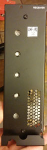
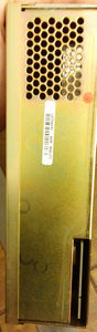
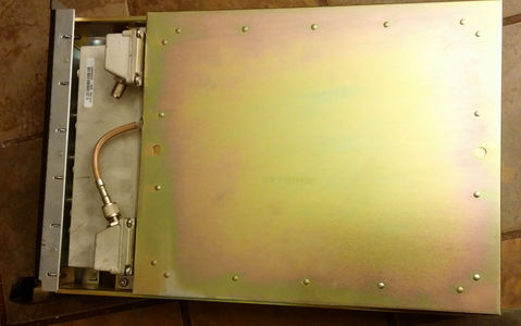
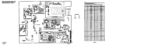
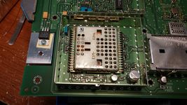
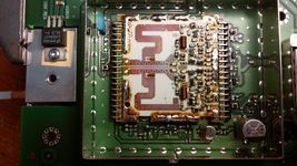
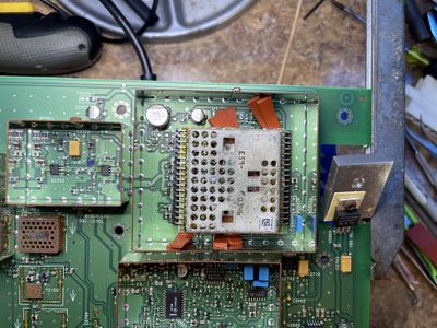
The basic receiver is pictured below. Note the UHF R1-R4 receivers have a preselector that's flush with the front panel and only 3 adjustment. This is a dead give away that you have a UHF R1-R4 from the front. Unfortunately there is not an easy way to identify it further than by part number.
UHF RX Front
UHF RX Back
UHF RX Case
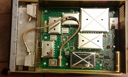
UHF RX Internal


The receiver is a high side injection with the 1st Lo operating +73.35 MHz higher than the receiver frequency.
The SCM knows what type of module is inserted by reading voltage divider resistors on the u2600 A/D Converter. Some of these are on ports used for other things, Change Frequency and Lock and then A8 input is used for ID. Note the resistors have the same labels on the UHF boards but on other bands the same parts have different labels. The R2606 and R2607 form a voltage divider feeding the A8 input with the computed voltage in volts.
| Range | R2449 Chg Freq | R2450 Lock | SPACE | R2606 | R2607 | A8 Volts |
|---|---|---|---|---|---|---|
| UHF R0 | 0 | 3300 | 5600 | 3300 | 1.9 | |
| UHF R1 | 0 | 0 | 1200 | 1200 | 2.5 | |
| UHF R2 | 0 | 3300 | 1200 | 1200 | 2.5 | |
| UHF R3 | 3300 | 0 | 1200 | 1200 | 2.5 | |
| UHF R4 | 3300 | 3300 | 1200 | 1200 | 2.5 | |
| VHF | R2413 | R2415 | R2812 | R2814 | ||
| VHF R1 | 0 | 0 | 2700 | 1200 | 1.5 | |
| VHF R2 | 0 | 3300 | 2700 | 1200 | 1.5 | |
| 800/900 | R2422 | R2414 | R2816 | R2815 | ||
| 900 | 0 | 0 | 1200 | 4700 | 4.0 | |
| 800 | 0 | 0 | 1200 | 2700 | 3.5 |
The service manual excerpt is in PDF and below.
UHF Receiver Models TRE6281-TRE6282-TRE6283-TRE6284 Service Manual Excerpt
In PNG format.
Schematic Sheet 1 of 4
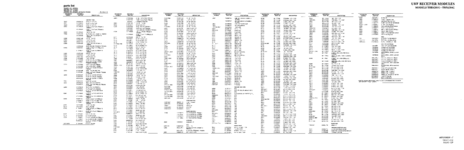
Schematic Sheet 2 of 4
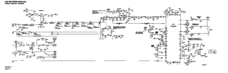
Schematic Sheet 3 of 4
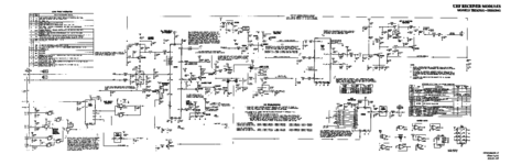
Schematic Sheet 4 of 4


Note on the schematic the VCO high and Low are reversed. This seems to be a recurring theme in the Quantar manuals.

As the VCO runs at 73.35 MHz higher than the intended receive frequency the VCO will expect to lock over the following ranges. The ideal spot for the VCO to operate is between 2.5 and 7.5 Volts highlighted in pink below.
| Range | Lower VCO | Upper VCO | ||||||||
|---|---|---|---|---|---|---|---|---|---|---|
| Volts | 0.8 | 2.5 | 5.0 | 7.5 | 9.2 | 0.8 | 2.5 | 5.0 | 7.5 | 9.2 |
| UHF R1 | 462 | 467 | 479 | 491 | 499 | 478 | 491 | 499 | 506 | 514 |
| UHF R2 | 498 | 511 | 519 | 527 | 536 | 514 | 527 | 535 | 543 | 552 |
| UHF R3 | 528 | 543 | 549 | 555 | 564 | 541 | 555 | 561 | 567 | 575 |
| UHF R4 | 553 | 567 | 574 | 580 | 589 | 568 | 580 | 587 | 593 | 601 |
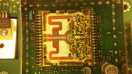
The VCO is much like the VCO in the exciter, a sealed unit with no further diagram available from the factory.
UHF R2 RX VCO Case on
UHF R2 RX VCO case off
UHF R2 VCO Close up


Conversions
Converting the boards
This is changing, I have a better way, old method.
R1 to R2
This is the conversion we're focused on as there are tons of 403-433 MHz (US Federal) Range 1 units on the market for cheap.
In general you should have the following to work on this:
- Soldering iron with fine tip (Metcal suggested)
- Hot air station
- Under board heater
- Small tools/tweezers
- Silicone rubber stock cut to support the underside of the VCO.
- Flux, and other small parts for rework
- Quantar backplane extender cables (PCI extender cables cut down to fit)
- A clear understanding of how the VCO's work and how the PLL operates
- Quantar programmed up with the test code plug.
Almost needed, you really should have it, but can do without:
- Voltmeter - You can use the WINRSS metering screen to view the steering level of the VCO. It's a pain to switch back and forth, but it can be done.
- Service monitor/SINAD meter - If you don't have a meter you can use a known weak signal to do a 20db quieting test.
- RJ-9 speaker to SINAD meter input cable.
Nice to have:
- Bench DVM
- Bench PSU
- Spectrum Analyzer and probes
Parts needed
You will need the following parts for this. Note the capacitors which are critical in terms of value are noted. If you find that sensitivity is off, suspect that you got the wrong value of caps here, 1-2 dB will be noticeable.
| Value | Tolerence | Part(s) | Digikey partnumber | Size |
|---|---|---|---|---|
| 3.3 | +-0.1pf 50v | C2070 | 732-12216 | 0805 |
| 5.6 | +-0.25pf 50v | C2076, C2079 | 478-KGM21BCG2A5R6CT-ND | 0805 |
| 6.8 | +-0.1pf 50v | C2054 | 478-KGM21BCG2A6R8DTCT-ND | 0805 |
| 8.2 | +-0.1pf 50v | C2050 | 732-12219-1-ND | 0805 |
| 13 | +-2pf 50v | C2051, C2059 | 478-10374-1-ND | 0805 |
| 16 | +-2pf 50v | C2053, C2057 | 478-10377-1-ND | 0805 |
| 22 | 5% 50v | C2083 | 478-KGM21BCG2A220JTCT-ND | 0805 |
| 3300 | 5% 1/8 watt | R2450 | RMCF0805JT3K30CT-ND | 0805 |
Procedure Overview
In general the VCO (both) need to be moved up in frequency and the image filters from the mixer need to be moved up by changing some chip caps. The ID resistors of the board must be changed to identify the receiver as Range 2 as well. Prior procedures required a bunch of manual power supplies, sweeping the circuit, and monitoring with a spectrum analyzer. This procedure uses the Quantar to control the receiver as it's being worked on using an extender cable.
The VCO must be modified so that it's able to lock from 2.5 to 7.5v. The steering voltage actually is usable from .95 to 8.95v, but tempeture will affect the resonance of the VCO, and so you want to have the high and low frequency to be at 2.5 - 7.5 volts giving enough room on each side for environmental variations.
Preparation
First lets prep the setup and get some notes on the receiver before we move it.
Setup the Quantar and install the extender cables.
Remove the receiver from it's housing.
Install the board in the work holder/vise.
Hook it up to the backplane and program in the Range 1 test codeplug.
Sweep and record the VCO steering voltage on each channel where it locks. If not using a voltmeter, you can use the measurement screen in RSS to see the steering level. This is very important as it gives a base line of performance on the receiver before modification.
Note that if you're using a volt meter on the VCO steering line, it will not receive properly. Ensure you do that separate from the SINAD testing.
| Lower VCO | Upper VCO | |||||||||||||||
|---|---|---|---|---|---|---|---|---|---|---|---|---|---|---|---|---|
| Channel | 1 | 2 | 3 | 4 | 5 | 6 | 7 | 8 | 9 | 10 | 11 | 12 | 13 | 14 | 15 | 16 |
| R1 | 384.5250 | 388.2250 | 391.9250 | 395.6250 | 399.3250 | 403.0250 | 410.5000 | 417.9750 | 418.0250 | 425.5000 | 432.9750 | 436.8000 | 440.6250 | 444.4500 | 448.2750 | 452.1000 |
| R2 | 417.9000 | 421.9250 | 425.9500 | 429.9750 | 434.0000 | 438.0250 | 446.0000 | 453.9750 | 454.0250 | 462.0000 | 469.9750 | 474.1250 | 478.2750 | 482.4250 | 486.5750 | 490.7250 |
| R1 Shield on | UNLOCK | UNLOCK | 1.813 | 2.504 | 3.248 | 4.029 | 5.678 | 7.379 | 3.843 | 5.495 | 7.204 | 8.089 | 8.982 | UNLOCK | UNLOCK | UNLOCK |
| R1 Shield Off | UNLOCK | 1.808 | 2.480 | 3.203 | 3.962 | 4.743 | 6.376 | 8.045 | 4.735 | 6.395 | 8.084 | 8.959 | UNLOCK | UNLOCK | UNLOCK | UNLOCK |
| Delta | 0.667 | 0.699 | 0.714 | 0.714 | 0.698 | 0.666 | 0.892 | 0.900 | 0.880 | 0.870 | ||||||
| R1 SINAD | -120.1 | -120.1 | -120.0 | -120.1 | -120.1 | -120.2 | -120.0 | -120.0 | -120.0 | -119.4 | 119.4 | |||||
| R2 Shield On | UNLOCK | UNLOCK | 1.328 | 2.056 | 2.876 | 3.766 | 5.680 | 7.727 | 2.319 | 4.001 | 5.890 | 6.920 | 7.968 | 9.027 | UNLOCK | UNLOCK |
| R2 SINAD | ||||||||||||||||
VCO Modification
This is very critical circuit to work on and is a sealed ceramic unit. Motorola used unique VCO's for each band range, however the Range 1 can be modified using some "stub" lines of copper foil to bring it's frequency up. This is complicated as the unit is soldered in place and has a heavy plated steel cover soldered over it.
Prepare the VCO for rework
The VCO shield must be removed, but as the entire VCO will be reflowed at the same time, it will "fall" off the headers holding it off the board. This is solved by using some 1/4 inch wide 60 mil thick silicone stock. Fold the small pieces under the VCO and compress them to provide some slight pressure between the bottom of the VCO and the top of the PCB. This works as the headers will not be reflowed and release from the PCB.
Silicone Supports
VCO with supports installed under board
VCO with case off and silicone strips


After this is done, flip the board over and unsolder the 4 posts of the shield that go to ground. I find the best way to do this is lots of flux and solder braid with a pre-heated board, but chip-quick solder will work to lower the melting point so that when the top reflows the ground will too. Either way will work.
Now flip the board back and let it pre-heat. A bit of insulation over the VCO will help for this. I set my pre-heater to 550f and let it rip for 5-10 min.

Set the hot air gun to 550F and 20 L/min of flow, slowly work the shield up in temp and test the solder melting around it. Once it's completely reflowed, lift up on the center of the shield and pull it directly up and clear of the PCB. Set it aside to cool. Careful you don't disturb any of the VCO parts, as they will most likely be reflowed. If you do, don't panic, just look at the before picture and put everything back to how it was on the VCO. It's a pretty easy circuit to figure out.
Before allowing the VCO to cool, tin the U portions of each VCO strip with solder and flux. Once this is done put the insulation over the VCO module and turn the pre-heater off, allow it to cool but not fast, as rapid changes can crack the ceramic PCB.
Modify the VCO
Power up the Quantar and the receiver. Ensure it's locked and you can read the steering voltages on the VCO. Now you need to program the Range 2 Test Codeplug into the quantar and let it reload. It should show up as receiver PLL unlocked when it boots, this is ok.
Prep two copper foil strips to 50 mil wide by .250 long. If the foil has adhesive on one side, remove it using some solvent.
Turn on the pre-heater and let it warm the VCO up, you will see the VCO voltage move as this happens.
VCO RULES
- Temp up = Volts up
- Temp down = Volts down
- Case off = Volts up
- Case on = Volts down
- Grinding the trim cap = Volts down
- Move short towards U = Volts up
- Move short away from U = Volts down
The concept is that we want the most tuning range from the VCO we can get, but that the 6-8 and 9-11 channels are all within 2.5-7.5v under normal operations once the VCO is reassembled.
First modify the lower VCO. This is best done on channel 7, as from solder hot temp to room temp, .75 to 1v higher is seen. Adding this to the +.7 to +.9v seen by removing the case, means we'll be adjusting the unit to almost 2v higher than it will be once reassembled. As we want to hit 7.5v at channel 8, we will run out of steering voltage trying to do that.
Set on channel 7 and solder the copper foil short over the lower VCO U bend in such a way that it shows 7.5v on the steering line. The VCO may unlock when hot, so solder it and then let it cool slightly to lock again. Blowing on it may help to lock back up. In practice it's better to have it slightly high as the stub can be ground with diamond grinder tool to shift the voltage down after it's assembled. Once you have the hang of it soldering it actually not hard.

Now to the upper VCO, and here we set to channel 9, and want 4.5v while hot. This may require bit more cooling to get it to lock between iterations, but it will lock easily.
Once the VCO is modified you can allow it to cool and test it more, or just reinstall the shield right now. If you allow it to cool, ensure you have the insulator on it while it cools, and record the shield off voltages before re-attaching the shield. If you do allow it to cool, use some solvent and remove all the flux from the VCO substrate. While flux residue shouldn't affect anything, it will look better and is more professional.
To reattach the shield, place the shield on the VCO and add a liberal amount of flux around it. Using the hot air gun to 550F and 20 L/min of flow reflow it and allow it to seat on the VCO. You may need to add some extra solder around the VCO shield, but typically there's more than enough to make it work. Once it's totally reflowed allow it to cool and solidify. As you need to solder the under side of the board, you can do that from the top, or flip it over and solder it.

Allow it all to cool using the insulator over the VCO again.
Test the VCO
Test the cooled VCO is locked across the channels 6-11, and note the voltage on channel 8 (Low VCO highest frequency) and channel 9 (high VCO lowest frequency), which should be 7.5 and 2.5 v respectively. If it's too high, you can grind the trimmer cap and bring it down, but within half a volt it is fine. If you'll be operating the station at tempeture extremums its more important, or if you intend to operate it out of the 438-470 MHz band.
Modify the image filters
Image filter under shield
The image filter under the shield needs to be modified, so the shield must be removed. This is done with the underboard pre-heater and 550f @ 20l/min of airflow. The shield will reflow and be easily removed.
It's best to prep the caps and have them ready as the parts under the shield will be reflowed when the shield is removed.
Remove C2050, 2051, 2053 and 2045 and replace them as follows:
| C2050 | 8.2 pF |
|---|---|
| C2051 | 13 pF |
| C2053 | 16 pF |
| c2054 | 6.8 pF |

Once this is done, re-solder the shield in place.
Image filter in mixer can
The image filter continues into the mixer can, but it's a pop off shield which is much easier to expose rather than a sealed unit.
Replace the following parts
Remove C2057, 2059, 2070, 2076, 2079 and 2083; replace them as follows:
| C2057 | 16pf pF |
| C2059 | 13 pF |
| C2070 | 3.3 pF |
| C2076 | 5.6 pF |
| C2079 | 5.6 pF |
| C2083 | 22 pF |

Change the Module ID
Change R2450 to a 3300 Ohm resistor. This will make the module be seen as an UHF R2 module by the SCM.

Clean board
I typically wash the board in some solvent/IPA or non-chlorinated brake cleaner and spray out the VCO. An acid brush or toothbrush might be needed to clean it up. After some rinses with clean solvent, bake it at 150f for 30 min and check that's it's clean.
Let it cool and move on to testing.
Test and Verify
Using the same method as before, note the final VCO voltage at each test frequency and the sensitivity. You should ideally see the same or within 1dB of performance depending on the stability of your test setup. Having the speaker connected helps as you'll be able to hear where it's at. The DSP does noise reduction, and with a steady weak signal, this can make it hard to test SINAD.
Useful Docs
Here is a complete list of the parts which are changed, color coded by section of the board.
| Part number | R1 | R2 | Notes |
|---|---|---|---|
| C2050 | 9.1 pF | 8.2 pf +-0.1pf | 5% is .41pf |
| C2051 | 16pF | 13pf +-2pf | 5% is .65 pf |
| C2053 | 18 pF | 16 pf +-2pf | 5% is .8 pf |
| C2054 | 8.2 pF | 6.8 pf +-0.1 pf | 5% is .34 pf |
| C2057 | 18 pF | 16 pf +- 2pf | 5% is .8 pf |
| C2059 | 18 pF | 13 pf +- 2pf | 5% is .65 pf |
| C2070 | 5.6 pF | 3.3 pF +- 0.1 pf | 5% is .165pf |
| C2076 | 7.54 pF | 5.6 pf +- 0.25pf | 5% is .28 pf |
| C2079 | 9.1 pF | 5.6 pf +- 0.25pf | 5% is .28 pf |
| C2083 | 47 pF | 22 pf 5% | |
| R2449 | 0 Ohm | 0 Ohm | ID Leave |
| R2450 | 0 Ohm | 3300 Ohm | ID Replace |
The following image has all the R1 to R2 mods on it and can be printed on a 8.5"x11" or A4 page to have a reference on the desk while doing this modification.

R3 to R2
This is possible, the VCO is the hard part as the frequency needs to be lowered. This means adding length to the resonator strip, which is in practice harder than the lower R1 where we need to remove length. This actually wasn't that bad to do in practice.
In testing it doesn't have the same sweep in terms of volts vs frequency that the R2 or R1 conversion has.
Parts changed
Below is a colored copy of the parts changed. The * parts are the same between R3 and R2.
| Part number | R3 | R2 | Notes |
|---|---|---|---|
| C2030 | 6.8 pF | 6.2 pF +- 0.25 pF | |
| C2033 | 100 pF | 56 pF 5% | |
| C2038 | 56 pF | 100 pF 5% | |
| C2040 | 3.3 pF | 5.6pF +-0.25 pF | |
| L2030 | 4.7 nH | 8.2 nH 5% | |
| L2032 | 8.2 nH | 12 nH 5% | |
| C2050* | 8.2 pF | 8.2 pf +-0.1pf | 5% is .41pf |
| C2051 | 8.2 pF | 13pf +-2pf | 5% is .65 pf |
| C2053 * | 16 pF | 16 pf +-2pf | 5% is .8 pf |
| C2054 | 4.7 pF | 6.8 pf +-0.1 pf | 5% is .34 pf |
| C2057* | 16 pF | 16 pf +- 2pf | 5% is .8 pf |
| C2059 | 9.1 pF | 13 pf +- 2pf | 5% is .65 pf |
| C2061 | 7.5 pF | 9.1 pF +-0.1pF | |
| C2070 | 2.2 pF | 3.3 pF +- 0.1 pf | 5% is .165pf |
| C2073 | 3.3 pF | 2.2 pF +-0.1pF | |
| C2076 | 2.2 pF | 5.6 pf +- 0.25pf | 5% is .28 pf |
| C2079 | NP | 5.6 pf +- 0.25pf | 5% is .28 pf |
| C2083 | 10 pF | 22 pf 5% | |
| C2084 | 3.3 pF | 1 pF +-0.1 pF | |
| R2449 | 3300 Ohm | 0 Ohm | |
| R2450 | 0 Ohm | 3300 Ohm |
R4 to R2
No data on this yet, may be doable VCO will be a problem.