Difference between revisions of "First Generation PA"
| Line 3: | Line 3: | ||
= Basics = | = Basics = | ||
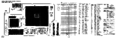
| − | The Basic module is pictured below | + | The Basic module is pictured below. |
| − | [[File:110W UHF PA layout.png| | + | [[File:110W UHF PA layout.png|300px|center|thumbnail|First Generation PA Layout]] |
| − | The complete | + | The major parts of the PA are |
| + | * Printed circuit board | ||
| + | * Intermediate PA | ||
| + | * Final PA | ||
| + | * Circulator | ||
| + | * Low Pass Filter | ||
| + | |||
| + | Each of these parts varies depending on the range of the PA. | ||
| + | {| class="wikitable sortable" | ||
| + | |- | ||
| + | ! Band !! IPA !! FPA !! Circulator !! LPF | ||
| + | |- | ||
| + | | R1 || TLE9150 || TTE6321 || 5884911T04 || TTE6331 | ||
| + | |- | ||
| + | | R2 || TLE9150 || TTE6322 || 5884911T04 || TTE6332 | ||
| + | |- | ||
| + | | R3 || TLE9160 || TTE6323 || 5884911T18 || TTE6334 | ||
| + | |- | ||
| + | | R4 || CLE6090 || TTE6342 || 5884911T18 || TTE6334 | ||
| + | |} | ||
| + | |||
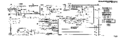
| + | The IPA module is a 10 W output that feeds into the FPA. Note the schematic diagram has some errors on it regarding a 30-35W output from the IPA. This is an error as it's from the 25W UHF PA diagram. | ||
| + | |||
| + | The FPA module consists of two parallel PA strips with two FET's each for a total of four devices. Each strip is addressed as "A" and "B" in the radio for the current monitoring of the PA. | ||
| + | |||
| + | Unfortunately there is no diagram of the IPA or FPA modules. | ||
| + | |||
| + | Note there is no CPU or even much digital circuitry in the PA. All metering is done via the exciter CPU mostly using an analog input and switches (U4103/4) to switch this input between different voltages on the PA. | ||
| + | |||
| + | The exciter controls the output power by an analog output (V_CONT) 0-5v from the CPU. This voltage is then used to control a couple transistors (Q4100 & Q4101) making the V_OMNI voltage that varies the first stage in the Intermediate PA. | ||
| + | |||
| + | |||
| + | The complete schematics are PNG format and are also available as a | ||
[[Media:110W UHF PA TTE2061A TTE2062B TTE2063 TTE2064.pdf|PDF]] | [[Media:110W UHF PA TTE2061A TTE2062B TTE2063 TTE2064.pdf|PDF]] | ||
<gallery> | <gallery> | ||
| Line 15: | Line 47: | ||
= Conversions = | = Conversions = | ||
| − | Converting from a R1 to R2 is quite easy | + | Converting from a R1 to R2 is quite easy. |
Revision as of 13:52, 15 November 2015
The Quantar First Generation UHF Power Amps cover UHF R1, R2, R3 and R4. R0, 380-433 MHz, was a slight redesign, and it is covered else where.
Basics
The Basic module is pictured below.

The major parts of the PA are
- Printed circuit board
- Intermediate PA
- Final PA
- Circulator
- Low Pass Filter
Each of these parts varies depending on the range of the PA.
| Band | IPA | FPA | Circulator | LPF |
|---|---|---|---|---|
| R1 | TLE9150 | TTE6321 | 5884911T04 | TTE6331 |
| R2 | TLE9150 | TTE6322 | 5884911T04 | TTE6332 |
| R3 | TLE9160 | TTE6323 | 5884911T18 | TTE6334 |
| R4 | CLE6090 | TTE6342 | 5884911T18 | TTE6334 |
The IPA module is a 10 W output that feeds into the FPA. Note the schematic diagram has some errors on it regarding a 30-35W output from the IPA. This is an error as it's from the 25W UHF PA diagram.
The FPA module consists of two parallel PA strips with two FET's each for a total of four devices. Each strip is addressed as "A" and "B" in the radio for the current monitoring of the PA.
Unfortunately there is no diagram of the IPA or FPA modules.
Note there is no CPU or even much digital circuitry in the PA. All metering is done via the exciter CPU mostly using an analog input and switches (U4103/4) to switch this input between different voltages on the PA.
The exciter controls the output power by an analog output (V_CONT) 0-5v from the CPU. This voltage is then used to control a couple transistors (Q4100 & Q4101) making the V_OMNI voltage that varies the first stage in the Intermediate PA.
The complete schematics are PNG format and are also available as a
PDF
Layout
Schematic Diagram
Conversions
Converting from a R1 to R2 is quite easy.